Chip splicing platform and chip splicing substrate leveling method

A chip and platform technology, applied in the field of chip splicing platform and chip splicing base plate leveling, can solve the problems affecting the flatness of the chip splicing surface, and achieve the effect of ensuring the flatness, improving the chip yield and improving the splicing efficiency.

Pending Publication Date: 2021-02-02
BEIJING SEMICON EQUIP INST THE 45TH RES INST OF CETC
View PDF6 Cites 1 Cited by
  • Summary
  • Abstract
  • Description
  • Claims
  • Application Information

AI Technical Summary

Problems solved by technology

[0003] The purpose of this application is to provide a chip splicing platform and a chip splicing substrate leveling method to solve the technical problem existing in the prior art that the plate base easily affects the flatness of the chip splicing surface

Method used


Image

  • Chip splicing platform and chip splicing substrate leveling method
  • Chip splicing platform and chip splicing substrate leveling method
  • Chip splicing platform and chip splicing substrate leveling method

Examples


Embodiment 1

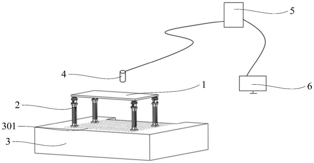
[0048] see figure 1 and figure 2 As shown, the embodiment of the present application provides a chip splicing platform, including:

[0049] Splicing the substrate 1 to form a splicing surface for supporting the chip;

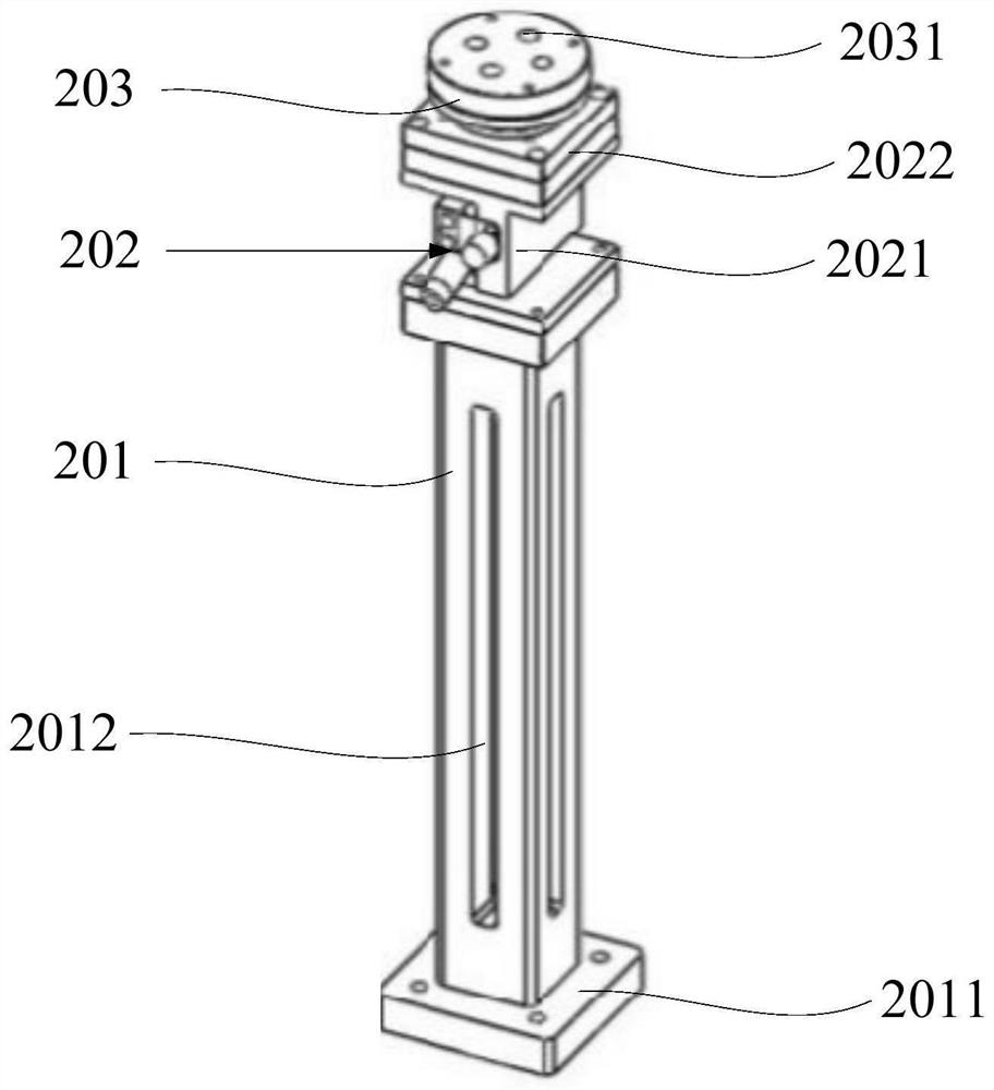
[0050] The leveling component is connected with the splicing base plate 1, and the leveling component has a retractable structure, and the leveling component is used to support the splicing base plate 1 and adjust the flatness of the splicing surface.

[0051]The chip splicing platform provided by this application includes a splicing base plate 1 and a leveling component, wherein the splicing base plate 1 is formed with a splicing surface for supporting chips, and the splicing of the chip is completed on the splicing surface, and the leveling component is in phase with the splicing base plate 1 The connection, the leveling component can support the splicing base plate 1, the part of the leveling component has a retractable structure, and the height of the lev...

Embodiment 2

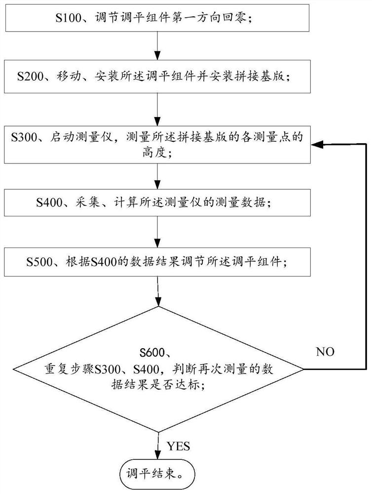
[0079] see image 3 As shown, Embodiment 2 of the present application also provides a chip splicing substrate leveling method, using the chip splicing platform described in the above-mentioned Embodiment 1, therefore, it has all the beneficial technical effects of the chip splicing platform, and the same technical features And the beneficial effects will not be repeated.

[0080] The chip splicing substrate leveling method provided in this embodiment specifically performs the following steps:

[0081] S100. Adjust the leveling assembly to return to zero in the first direction;

[0082] Specifically, select an appropriate number of leveling units according to the size of the splicing substrate, and restore the driving end of the driving device of each leveling unit of the adjustment assembly to the initial position, so that the self-adaptive leveling module is in the initial state, so that the leveling assembly is in the initial state. The lifting amount in the third directio...


PUM


Abstract

The invention relates to the technical field of semiconductors, in particular to a chip splicing platform and a chip splicing substrate leveling method. The chip splicing platform comprises: a splicing substrate, which is provided with a splicing surface and is used for supporting a chip; and a leveling assembly, which is connected with the splicing substrate, is provided with a telescopic structure, and is used for supporting the splicing substrate and adjusting the flatness of the splicing surface. According to the chip splicing platform provided by the invention, the flatness of the splicing surface of the splicing substrate can be adjusted by adjusting the leveling assembly, so the splicing surface is close to be horizontal to the greatest extent, the flatness of a spliced chip is ensured, splicing efficiency is improved, and chip yield is increased.

Description

technical field [0001] The present application relates to the technical field of semiconductors, in particular to a chip splicing platform and a chip splicing substrate leveling method. Background technique [0002] At present, chip splicing has very strict requirements on the flatness of the chip surface after splicing. Therefore, there are very high requirements on the flatness of the splicing substrate installation before chip splicing. Before splicing, the substrate needs to be leveled with high precision. The existing splicing equipment usually places the base plate directly on the plate holder, which has high requirements on the flatness of the plate itself, and it is difficult to guarantee the flatness of the large-size plate base. Therefore, this method has a certain degree of It affects the surface flatness of chip splicing, and this effect is difficult to eliminate. Contents of the invention [0003] The purpose of this application is to provide a chip splicing ...

Claims


Application Information

Patent Timeline
Patent Type & Authority Applications(China)
IPC IPC(8): H01L21/67
CPCH01L21/67121H01L21/67132H01L21/67253
Inventor 高慧莹党景涛许向阳王河刘路宽
Owner BEIJING SEMICON EQUIP INST THE 45TH RES INST OF CETC
Why Eureka
Try Eureka