Semiconductor assembly and manufacturing method thereof

A manufacturing method and semiconductor technology, applied in semiconductor devices, semiconductor/solid-state device components, electric solid-state devices, etc., can solve the problems of multi-chip area, occupancy, yield loss, etc.

Pending Publication Date: 2021-02-05
WINBOND ELECTRONICS CORP
View PDF7 Cites 0 Cited by
  • Summary
  • Abstract
  • Description
  • Claims
  • Application Information

AI Technical Summary

Problems solved by technology

[0003] When the wafer is cut, cracks may occur due to the stress of the saw blade. Therefore, a sealing ring is usually formed around the chip to prevent cracks from extending to the chip area and damaging the internal circuit, resulting in loss of yield.
However, the seal ring or the area between the seal ring and the chip area may take up too much chip area

Method used


Image

  • Semiconductor assembly and manufacturing method thereof
  • Semiconductor assembly and manufacturing method thereof
  • Semiconductor assembly and manufacturing method thereof

Examples


Embodiment Construction

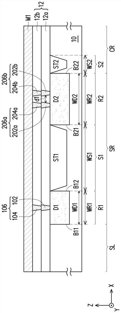
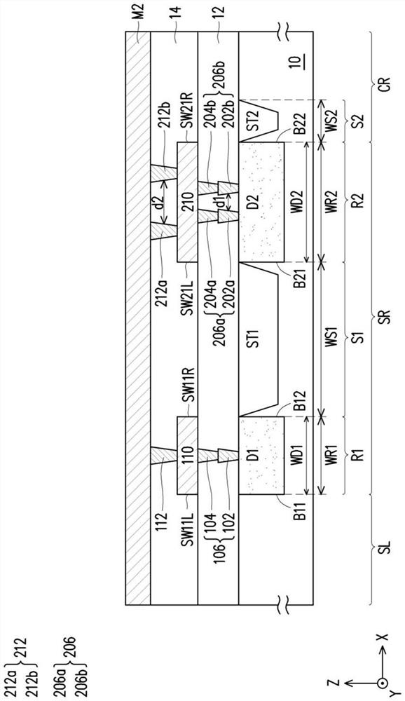
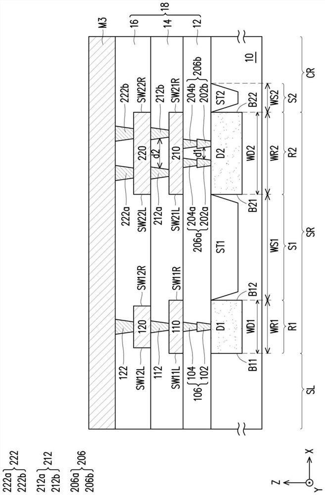
[0024] Please refer to Figure 1A , providing a substrate 10 . The substrate 10 may be a semiconductor substrate 10 . The substrate 10 may include a chip region CR, a seal ring region SR and a cutting region SL. The chip region CR may be used to form electronic components. The cutting area SL surrounds the chip area CR. During the subsequent singulation step, cleavage can be performed along the cleavage zone SL. The seal ring area SR is located between the chip area CR and the cutting area SL. A sealing ring can be formed in the sealing ring region SR, and can prevent the cracks generated by dicing the wafer from extending to the chip region CR and damaging the electronic components in the chip region CR during the subsequent singulation step.

[0025] A plurality of isolation structures ST1 and ST2 are formed in the chip region CR and the sealing ring region SR. The isolation structure is, for example, a shallow trench isolation structure.

[0026] The width WS1 of the...


PUM


Abstract

The invention provides a semiconductor assembly and a manufacturing method thereof. The manufacturing method comprises the following steps: forming a first sealing ring and a second sealing ring whichare separated from each other on a substrate; forming a protective layer on the substrate for covering the first sealing ring and the second sealing ring, wherein the portion, between the first sealing ring and the second sealing ring, of the protective layer is provided with a concave surface; removing the protective layer at the concave surface and a part of the protective layer on the first sealing ring, forming a gap wall on the side wall of the first sealing ring, and forming an opening in the protective layer, wherein the width of the opening is greater than that of the first sealing ring, and the opening enables the top surface of the first sealing ring and the clearance wall to be exposed.

Description

technical field [0001] The invention relates to an integrated circuit and its manufacturing method, in particular to a semiconductor component and its manufacturing method. Background technique [0002] With the advancement of science and technology, all kinds of electronic products are developing towards the trend of high speed, high performance, light weight and short size. How to effectively use the chip area and improve the yield rate is a very important issue at present. [0003] When the wafer is diced, cracks may occur due to the stress of the dicing saw blade. Therefore, a sealing ring is usually formed around the chip to prevent the crack from extending to the chip area and damaging the internal circuit, resulting in a loss of yield. However, the seal ring or the area between the seal ring and the chip area may occupy too much chip area. Contents of the invention [0004] The embodiment of the present invention provides a method for manufacturing a semiconductor...

Claims


Application Information

Patent Timeline
Patent Type & Authority Applications(China)
IPC IPC(8): H01L23/00
CPCH01L23/562
Inventor 蔡耀庭陈江宏庄哲辅洪文
Owner WINBOND ELECTRONICS CORP
Why Eureka
Try Eureka