
Manufacturing method of 8-shaped blind hole of printed circuit board

A technology for printed circuit boards and manufacturing methods, applied in the directions of printed circuit manufacturing, printed circuits, electrical components, etc., can solve the problems of small blind hole diameter, thin dielectric layer thickness, separation, etc.

Active Publication Date: 2021-02-05
DYNAMIC ELECTRONICS KUNSHAN
View PDF5 Cites 0 Cited by
  • Summary
  • Abstract
  • Description
  • Claims
  • Application Information

AI Technical Summary

Problems solved by technology

[0002] In the traditional blind hole laser processing technology, the aperture of the laser blind hole is generally small, and the thickness of the dielectric layer is thin. For CO 2 Laser processing is easier to process; for some millimeter-wave radars, it is necessary to open irregular laser blind holes ("8"-shaped blind holes) on the PCB (printed circuit board), and the blind hole aperture and dielectric layer thickness are larger than the traditional blind hole aperture. And the thickness of the dielectric layer increases, so it brings many technical difficulties to the production
[0003] In the traditional blind hole laser processing technology, due to the small diameter of the blind hole and the thin thickness of the dielectric layer, the CO 2 Laser processing is also easy to process under the premise of meeting the quality requirements; the irregular blind hole ("8" shaped blind hole) design, there will be some overlapping areas between the two blind holes, and the traditional processing method will cause the overlapping area to be repeatedly lasered Processing causes the bottom of the blind hole to be broken down or the copper at the bottom of the blind hole is separated from the bonding sheet, so it is a technical problem in the blind hole laser processing process

Method used


Image

  • Manufacturing method of 8-shaped blind hole of printed circuit board

Examples


Embodiment

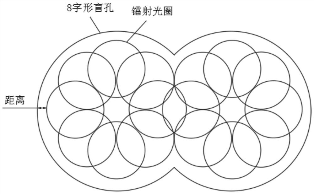
[0035] Embodiment: A kind of manufacturing method of 8-shaped blind hole of printed circuit board comprises the following steps:

[0036] S1. Cutting: cut the base plate to a suitable size, and bake it in an oven at 120-170°C for 2-4 hours to release the internal stress of the base plate;

[0037] S2. Inner layer circuit: Etch the inner layer circuit. After the inner layer circuit is made, scan the board surface with an optical inspection machine to ensure that there is no gap on the PAD at the bottom of the circuit / blind hole;

[0038] S3. Outer layer copper window: Etch out the required blind hole diameter by opening the copper window. The compensation method of the copper window is to compensate the aperture size according to the copper thickness. When the copper thickness is 8mil, the diameter of the copper window opening needs to be increased by 1mil ;

[0039] S4. Laser laser: The blind hole is burned out by laser laser copper window. When the copper window is laser pro...


PUM


Abstract

The invention discloses a manufacturing method for an 8-shaped blind hole of a printed circuit board. The method comprises the following steps of: cutting, etching an inner-layer circuit, etching theaperture of the required blind hole in a copper window opening mode, exposing the blind hole in a laser copper window opening mode, and extending energy to the periphery in the processing process dueto the fact that the size of an aperture is larger than that of the aperture during laser processing of the copper window. The 8-shaped blind hole is manufactured in a laser winding mode, the distancebetween the edge position of a laser aperture and the round edge of a copper window is controlled to be 0.5-1.0 mil, acid etching is conducted after electroplating, in the acid etching process, a blind hole area and a circuit are protected by a dry film, and before acid etching, the dry film of a non-blind hole and the dry film of a circuit area are stripped through a developing process, a coppersurface is exposed and etched by an etching liquid, and finally optical inspection and resistance test are implemented. By means of the method, repeated laser machining of the overlapping area between the two blind holes can be prevented, and the machining quality of the 8-shaped blind hole is guaranteed.

Description

technical field [0001] The invention belongs to the technical field of printed circuit boards, in particular to a method for manufacturing a figure-eight blind hole of a printed circuit board. Background technique [0002] In the traditional blind hole laser processing technology, the aperture of the laser blind hole is generally small, and the thickness of the dielectric layer is thin. For CO 2 Laser processing is easier to process; for some millimeter-wave radars, it is necessary to open irregular laser blind holes ("8"-shaped blind holes) on the PCB (printed circuit board), and the blind hole aperture and dielectric layer thickness are larger than the traditional blind hole aperture. And the thickness of the dielectric layer increases, so it brings many technical difficulties to the production. [0003] In the traditional blind hole laser processing technology, due to the small diameter of the blind hole and the thin thickness of the dielectric layer, the CO 2 Laser pro...

Claims


Application Information

Patent Timeline
Patent Type & Authority Applications(China)
IPC IPC(8): H05K3/00C25D7/00C25D3/38C23F1/18
CPCH05K3/0017H05K3/0035C25D3/38C25D7/00C23F1/18
Inventor 黄铭宏
Owner DYNAMIC ELECTRONICS KUNSHAN
Learn More