Integrated circuit layout method

A technology of integrated circuits and layout methods, applied in CAD circuit design, electrical digital data processing, special data processing applications, etc., can solve problems such as rising leakage, not necessarily good results, and time-consuming

Pending Publication Date: 2021-02-09
REALTEK SEMICON CORP
View PDF0 Cites 0 Cited by
  • Summary
  • Abstract
  • Description
  • Claims
  • Application Information

AI Technical Summary

Problems solved by technology

[0003] As mentioned above, manually moving the components in the circuit may cause problems in the originally converged timing and/or leakage power problems. The subsequent correction process will not only increase the circu

Method used


Image

  • Integrated circuit layout method
  • Integrated circuit layout method
  • Integrated circuit layout method

Examples


Embodiment Construction

[0012] The terms used in the following explanations refer to the customary terms in the technical field. If some terms are explained or defined in this manual, the explanations of these terms shall be based on the descriptions or definitions in this manual.

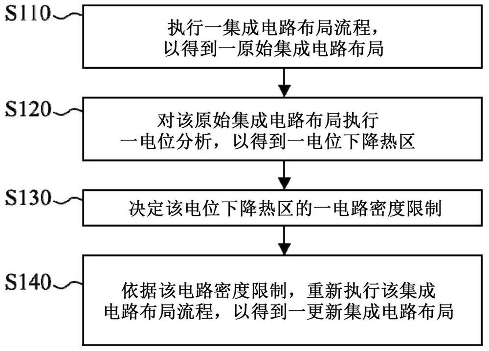
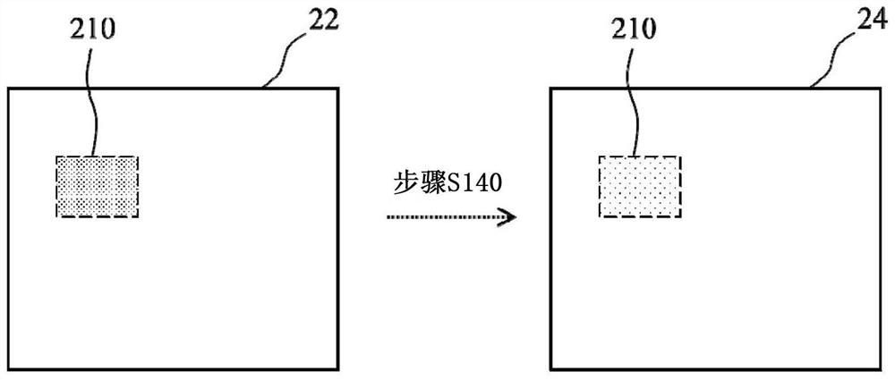
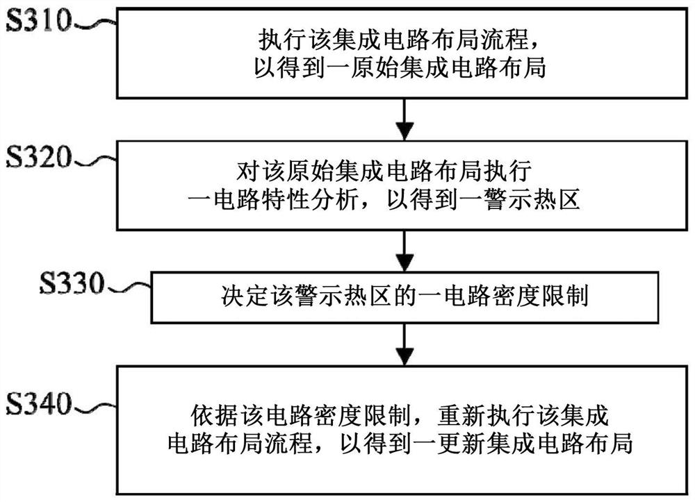
[0013] The invention discloses an integrated circuit layout method, which can improve the circuit characteristics of the result of an integrated circuit layout process, and can reduce manpower intervention, so as to improve and speed up the integrated circuit layout process. The present invention is applicable to the design process of an application-specific integrated circuit (ASIC) or other types of integrated circuits, and is especially suitable for the design of integrated circuits (such as: high-speed and low-power integrated circuits) sensitive to potential drop (IR Drop) process; however, the application of the present invention is not limited thereto.

[0014] figure 1 An embodiment of the integrated circuit layo...


PUM


Abstract

The invention discloses an integrated circuit layout method, which can reduce the potential drop of the result of an integrated circuit layout process, and comprises the following steps of: executingthe integrated circuit layout process to obtain an original integrated circuit layout; performing a potential analysis on the original integrated circuit layout to obtain a potential drop hot zone; determining a circuit density limit of the potential drop hot zone; and re-executing the integrated circuit layout process according to the circuit density limit to obtain an updated integrated circuitlayout.

Description

technical field [0001] The present invention is a method of circuit layout, and more particularly relates to a method of layout of an integrated circuit. Background technique [0002] In the design process of integrated circuits (such as application-specific integrated circuits (ASICs)), engineers will perform potential drop (IR drop) verification on circuits after timing closure (timing closure) before chip tape-out, in order to To ensure the stability of the circuit performance or the internal circuit of the chip will not be overheated. Due to the layout of certain components (for example: standard cells with large volume, strong thrust and concentrated distribution, or standard cells with small thrust driven by specific signal patterns), the potential drop problem is likely to occur, Manually adjusting the positions of these components or reducing the size (size-down) in the circuit after timing convergence is to solve the above problems by dispersing and reducing the lo...

Claims


Application Information

Patent Timeline
IPC IPC(8): G06F30/392G06F115/06
Inventor 林殿国林立镒张云智
Owner REALTEK SEMICON CORP
Why Eureka
Try Eureka