Semiconductor integrated circuit

a technology of integrated circuits and semiconductors, applied in the direction of amplifiers with semiconductor devices/discharge tubes, basic electric elements, solid-state devices, etc., can solve the problems of deterioration of high frequency characteristics, loss of desired circuit characteristics, and deterioration of circuit characteristics, so as to avoid the problem of multi-layer interconnection and improve circuit characteristics.

Inactive Publication Date: 2005-11-22
SEMICON COMPONENTS IND LLC
View PDF10 Cites 0 Cited by
  • Summary
  • Abstract
  • Description
  • Claims
  • Application Information

AI Technical Summary

Benefits of technology

[0015]This invention is directed to solve the problems addressed above, by assigning each of a plurality of interconnection layers to each of interconnection purposes in designing an integrated circuit having a circuit block with a plurality of semiconductor elements and multi-layer interconnections at least to connect the semiconductor elements. Complicating the multi-layer interconnection can be avoided with the invention, leading to improved circuit characteristics.

Problems solved by technology

Attention is paid to secure pair matching of the transistors Q11 and Q12 as well as pair matching of the load resistors R1 and R12, since a midpoint potential of the output would shift, resulting in a loss of desired circuit characteristics, if balance between elements is lost.
However, even though attention is paid to secure the pair matching of the transistors Q11 and Q12 as well as pair matching of the load resistors R11 and R12 in the above mentioned circuit, there are problems, which are described below, when the circuit is laid out to dispose each of the semiconductor elements according to a circuit diagram, for instance from left to right (or from right to left).
Therefore, pair matching of the semiconductor integrated circuit which includes the differential amplifier 11 could be lost, and an impedance offset could arise when the circuit blocks are interconnected, resulting in deterioration in the circuit characteristics.
High frequency characteristics are deteriorated due to signal cross talk when the interconnections intersect with each other.
Therefore, when the circuit blocks are interconnected, desired characteristics might not be obtained because of the offset due to the impedance.
In the integrated circuit of the prior art, because rules (purpose of usage and pair matching) have not been established for each layer of the interconnections, each of interconnections are formed with a different layer taking the easy way out when the intersection of the interconnections is expected, thus causing deterioration in the circuit characteristics.
However, when the interconnection is made based on the criteria mentioned above (such as using the first layer metal for horizontal interconnection and using the second layer metal for vertical interconnection), a plurality of interconnection layers is used even where a single layer of interconnection could make the interconnection, making the interconnection too complicated.

Method used


Image

  • Semiconductor integrated circuit
  • Semiconductor integrated circuit
  • Semiconductor integrated circuit

Examples


Embodiment Construction

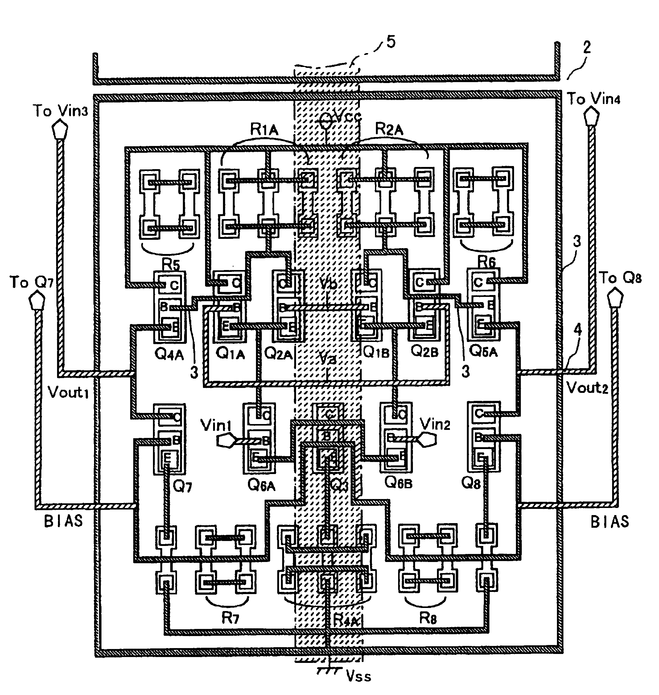
[0023]An embodiment of a semiconductor integrated circuit of this invention will be explained referring to the figures.

[0024]The explanation will be given by taking a differential amplifier, which is frequently used in bipolar linear integrated circuit, as an example.

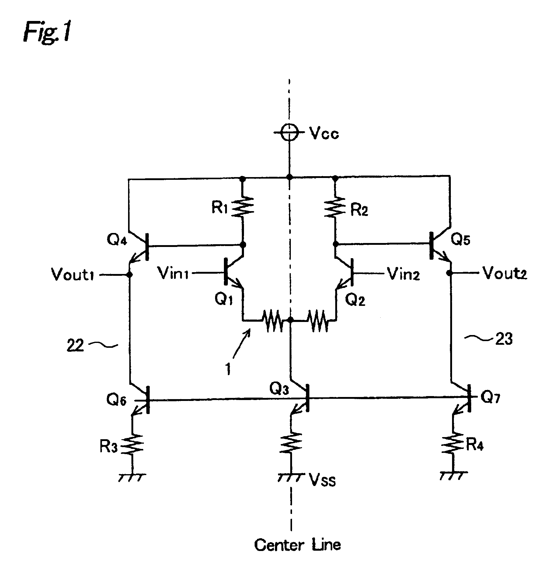
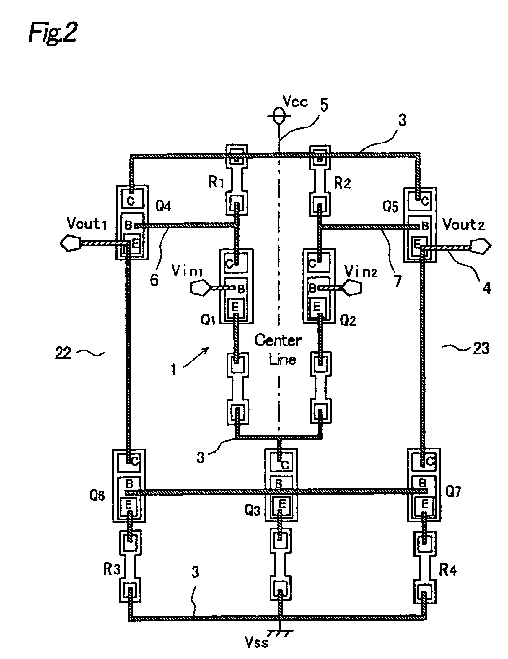
[0025]As shown in FIG. 1, each of a pair of emitter follower circuits 22 and 23 is connected respectively to each of a pair of differential output terminals of a circuit block 1 (a differential amplifier in this embodiment) composed of bipolar transistors. The emitter follower circuits 22 and 23 are disposed symmetrically with respect to a center line of the circuit block 1.

[0026]Circuit pair matching is improved herewith compared to the conventional circuit shown in FIG. 6B, in which the emitter follower circuits 42 and 43 connected with a pair of the outputs of the differential amplifier 11 are disposed asymmetrically with respect to the center line of the differential amplifier 11. Therefore, the characteristics of a...


PUM


Abstract

A layout method of a semiconductor integrated circuit is provided which improves characteristics of the circuit by giving hierarchical structure of interconnections regularity. A pair of emitter followers is disposed symmetrically with respect to a center line of a differential amplifier. Thus, interconnections within a circuit block and a ground wiring can be made with a single metal layer, since an area where the interconnections cross with each other is eliminated. Herewith cross talk due to the intersection of the interconnections can be resolved. Also, the interconnections between the differential amplifier and the emitter follower circuits can be made equal in length. It is possible to assign a second metal layer to interconnections between circuit blocks and a third metal layer to a power supply so that characteristics of the semiconductor integrated circuit are improved.

Description

BACKGROUND OF THE INVENTION[0001]1. Field of the Invention[0002]This invention relates to a semiconductor integrated circuit, specifically to a technology for structuring a circuit to improve characteristics of the circuit by giving regularity to a hierarchical structure of interconnections in a hierarchical design having multi-layer interconnections.[0003]2. Description of the Related Art[0004]A prior art semiconductor integrated circuit structure will be explained referring to FIGS. 6A and 6B hereinafter. The explanation will be given by taking a differential amplifier, which is frequently used in bipolar linear integrated circuits, as an example.[0005]In the basic structure of the differential amplifier 11, both emitters of a first transistor Q11 and a second transistor Q12 are connected to a constant current transistor Q13, and each of the collectors of the transistors Q11 and Q12 is connected to a power supply Vcc through load resistors R11 and R12, respectively, as shown in FI...

Claims


Application Information

Patent Timeline
Patent Type & Authority Patents(United States)
IPC IPC(8): H01L27/02H03F3/45
CPCH01L27/0207H03F3/45089H03F2203/45352H03F2203/45392H03F2203/45722H03F3/45
Inventor SHIINA, MASAHIRO
Owner SEMICON COMPONENTS IND LLC
Why Eureka
Try Eureka