
Self-reference storage structure and storage and calculation integrated circuit

A storage structure and self-referencing technology, applied in the field of memory, can solve the problems of low magnetic tunnel junction tunneling magneto-resistance, disadvantageous circuit integration, and low read margin.

Active Publication Date: 2021-02-19
INST OF MICROELECTRONICS CHINESE ACAD OF SCI
View PDF5 Cites 3 Cited by
  • Summary
  • Abstract
  • Description
  • Claims
  • Application Information

AI Technical Summary

Problems solved by technology

[0002]The core storage unit of magnetic random access memory (MRAM) is a magnetic tunnel junction. The magnetization reversal of this magnetic tunnel junction needs to add an external magnetic field, and the magnetic tunnel junction tunnels the magnetic The resistance is relatively low. Therefore, the existing memory is not only not conducive to circuit integration, but also causes high power consumption of the device during the writing process and low read margin.

Method used


Image

  • Self-reference storage structure and storage and calculation integrated circuit
  • Self-reference storage structure and storage and calculation integrated circuit
  • Self-reference storage structure and storage and calculation integrated circuit

Examples


Embodiment 1

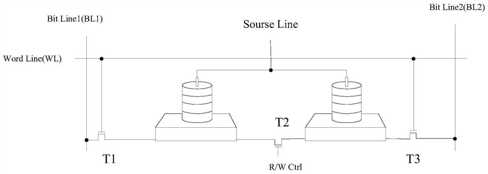
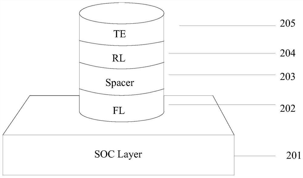
[0058] Embodiments of the present invention provide a self-referencing storage structure, such as figure 1 As shown, it includes: three transistors, including: a first transistor T1, a second transistor T2, and a third transistor T3; two magnetic tunnel junctions, including: a first magnetic tunnel junction MTJ0, a second magnetic tunnel junction MTJ1; a first The magnetic tunnel junction MTJ0 is connected in series between the first transistor T1 and the second transistor T2; the word line WL; the second magnetic tunnel MTJ1 junction is connected in series between the second transistor T2 and the third transistor T3; the first gate of the first transistor T1 Both the pole and the third gate of the third transistor T3 are connected to the word line WL; when the first transistor T1, the second transistor T2, and the third transistor T3 are turned on, the writing of one-bit binary information is realized.

[0059] Among them, such as figure 2 As shown, the first magnetic tunne...

Embodiment 2

[0089] An embodiment of the present invention provides an integrated storage and calculation circuit, such as Figure 6 As shown, it includes: a storage unit 601 , an asymmetric sense amplifier 602 and a voltage generating circuit 603 .

[0090] The storage unit 601 includes a plurality of parallel self-reference storage structures, and the storage unit generates a voltage difference between an induced voltage and a reference voltage under the action of a current.

[0091] The asymmetric sense amplifier 602 includes two transistors of different sizes.

[0092] The voltage generating circuit 603 is connected between the storage unit 601 and the asymmetric sense amplifier 602, and is used for inputting the voltage difference between the induced voltage and the reference voltage into the asymmetric sense amplifier 602, so as to realize a high read margin Data reading and logical operation functions.

[0093] Take gating a set of self-referencing storage structures as an example...


PUM


Abstract

The invention relates to the technical field of memories, in particular to a self-reference storage structure and a storage and calculation integrated circuit, and the self-reference storage structurecomprises: three transistors including a first transistor, a second transistor and a third transistor; and two magnetic tunnel junctions that comprise a first magnetic tunnel junction and a second magnetic tunnel junction; the first magnetic tunnel junction is connected in series between the first transistor and the second transistor; the second magnetic tunnel junction is connected in series between the second transistor and the third transistor; when the first transistor, the second transistor and the third transistor are started, write-in of one-bit binary information is realized; when data storage is realized, one-bit binary writing can be realized only by applying one-way current, and the device is low in time delay, low in power consumption and high in data reading margin in the writing process.

Description

technical field [0001] The invention relates to the technical field of memory, in particular to a self-referencing memory structure and a memory-computing integrated circuit. Background technique [0002] The core storage unit of Magnetic Random Access Memory (MRAM) is a magnetic tunnel junction. The magnetization reversal of the magnetic tunnel junction needs to add an external magnetic field, and the tunneling magnetoresistance of the magnetic tunnel junction is relatively low. Therefore, the existing memory is not only unfavorable for circuit integration. , Moreover, the writing process causes high power consumption of the device and low reading margin. [0003] Therefore, how to obtain a memory with low power consumption, low latency and high read margin is a technical problem to be solved urgently. Contents of the invention [0004] In view of the above problems, the present invention is proposed to provide a self-referencing memory structure and a memory-computing i...

Claims


Application Information

Patent Timeline
IPC IPC(8): G11C11/16
CPCG11C11/161G11C11/1659G11C11/1673G11C11/1675G11C11/1655G11C11/1693G11C11/5607G11C7/065
Inventor 邢国忠林淮刘宇张凯平张康玮吕杭炳谢常青刘琦李泠刘明
Owner INST OF MICROELECTRONICS CHINESE ACAD OF SCI
Learn More