Pick-and-place device for automatic wafer unloading

A pick-and-place device and wafer technology, which is applied in transportation and packaging, electrical components, semiconductor/solid-state device manufacturing, etc. , The effect of stable conveying and avoiding over-positioning phenomenon

Active Publication Date: 2021-02-26
SHANDONG NOVOSHINE OPTOELECTRONICS CO LTD
View PDF13 Cites 1 Cited by
  • Summary
  • Abstract
  • Description
  • Claims
  • Application Information

AI Technical Summary

Problems solved by technology

[0005] Specifically, the technical problem to be solved by the present invention is to provide a pick-and-place device for automatic unloading of wafers to solve the time-consuming and labor-intensive task of picking up slices during manual unloading, the efficiency of picking up slices is low, and the wafers are easy to be scratched. Technical Issues Affecting Wafer Quality

Method used


Image

  • Pick-and-place device for automatic wafer unloading
  • Pick-and-place device for automatic wafer unloading
  • Pick-and-place device for automatic wafer unloading

Examples


Embodiment Construction

[0046] The present invention will be further described below in conjunction with specific examples. However, the uses and purposes of these exemplary embodiments are only used to illustrate the present invention, and do not constitute any form of limitation to the actual protection scope of the present invention, nor limit the protection scope of the present invention thereto.

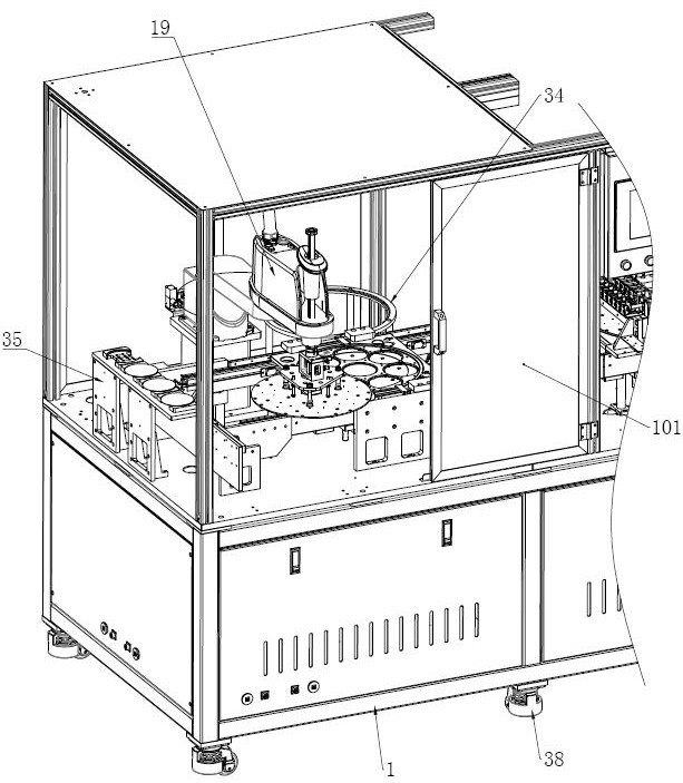
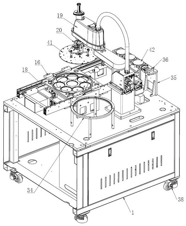
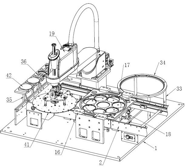
[0047] Such as Figure 1 to Figure 4 As shown, this embodiment provides a pick-and-place device for automatic unloading of wafers, including a frame 1, which is provided with a double-speed chain conveyor line, a carrier positioning mechanism, a pick-and-place robot arm 19, and a cover plate Table and wafer placement table, the carrier positioning mechanism is located between the two double-speed chains of the double-speed chain conveying line, the double-speed chain conveying line is provided with a blocking cylinder 18, and the blocking cylinder 18 is provided with two along the conveying direction o...


PUM


Abstract

The invention belongs to the technical field of wafer unloading and provides a taking and placing device for automatic wafer unloading. The taking and placing device comprises a rack, a speed chain conveying line, a carrier positioning mechanism, a taking and placing mechanical arm, a cover plate placing table and a wafer placing table are arranged on the rack, wherein a blocking cylinder is arranged on the speed chain conveying line; the taking and placing mechanical arm and the cover plate placing table are both located on one side of the speed chain conveying line, a taking and placing mechanism is arranged at the shaft end of the taking and placing mechanical arm, and the wafer placing table is located at one end of the speed chain conveying line; the material taking and placing mechanism comprises an installation frame installed on a working shaft of the taking and placing mechanical arm, a Bernoulli suction cup driven by a piece taking air cylinder is installed on the installation frame, a suction nozzle installation plate is further installed at the bottom of the installation frame, and a plurality of cover plate suction nozzles are installed at the bottom of the suction nozzle installation plate. Compared with a traditional manual wafer taking mode, wafer taking efficiency is greatly improved, the phenomenon that the wafer is accidentally scratched in the wafer discharging process is effectively avoided, and it is guaranteed that the quality and the percent of pass of the wafer are not affected in the wafer discharging process.

Description

technical field [0001] The invention relates to the technical field of wafer unloading, in particular to a pick-and-place device for automatic wafer unloading. Background technique [0002] Wafer refers to the silicon wafer used to make silicon semiconductor integrated circuits. Because of its circular shape, it is called a wafer. During the production and processing of wafers, according to the requirements of the processing technology, the wafers need to be arranged and placed in the wafer tray, and then the entire tray carrying the wafers is placed in a plasma etching machine for ICP etching. After the ICP etching process, the wafers are sequentially taken out from the wafer tray for subsequent AFM tests, etc. The process of taking the wafer out of the wafer tray is called wafer unloading. [0003] At present, the unloading operation of wafers in the tray is usually done manually. When unloading, the cover plate is first removed from the carrier plate, and then the wafers...

Claims


Application Information

Patent Timeline
Patent Type & Authority Applications(China)
IPC IPC(8): H01L21/677
CPCH01L21/67742H01L21/6776H01L21/67766H01L21/67775
Inventor 王子龙李凯杰陈仁明李健赵文文
Owner SHANDONG NOVOSHINE OPTOELECTRONICS CO LTD
Why Eureka
Try Eureka