Three-dimensional memory and preparation method thereof

A memory, three-dimensional technology, applied in the direction of electric solid-state devices, semiconductor devices, electrical components, etc., can solve the problems of gate layer breakdown, gate layer short circuit, etc.

Pending Publication Date: 2021-03-09
YANGTZE MEMORY TECH CO LTD
View PDF0 Cites 5 Cited by
  • Summary
  • Abstract
  • Description
  • Claims
  • Application Information

AI Technical Summary

Problems solved by technology

[0005] In view of the above-mentioned shortcomings of the prior art, the purpose of the present invention is to provide a three-dimensional memory and its manufacturing method, which is used to solve the problem of gate layer br

Method used


Image

  • Three-dimensional memory and preparation method thereof
  • Three-dimensional memory and preparation method thereof
  • Three-dimensional memory and preparation method thereof

Examples


Embodiment 1

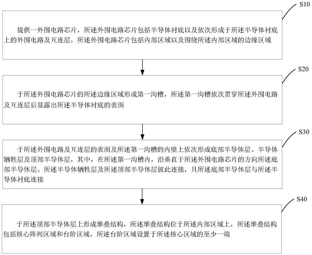
[0164] figure 1 The preparation flow chart of the three-dimensional memory of the embodiment of the present invention is shown, and the three-dimensional memory is based on the Under Core Arby, the PUC) architecture, that is, the peripheral circuit chip is located below the stacked structure. See figure 1 The three-dimensional memory preparation method comprises:

[0165] Step S10 provides an peripheral circuit chip, the peripheral circuit chip including a semiconductor substrate and an peripheral circuit and an interconnect layer sequentially formed on the semiconductor substrate, the peripheral circuit chip including an internal region and surrounding the internal region. Edge area;

[0166] Step S20 is formed in the edge region of the peripheral circuit chip, which is sequentially through the peripheral circuit and the interconnect layer revealed the surface of the semiconductor substrate;

[0167] Step S30, in the surface of the peripheral circuit and the interconnect layer...

Embodiment 2

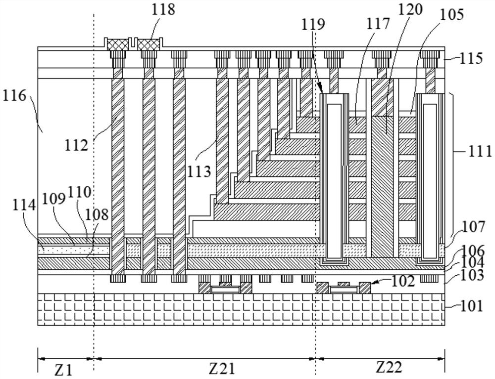
[0196] See Figure 16-19 The present invention also provides a three-dimensional memory prepared by the preparation method in the first embodiment, and the three-dimensional memory comprises at least a peripheral circuit chip, and a bottom semiconductor layer 206 formed on the peripheral circuit chip, an intermediate semiconductor layer, a top semiconductor layer. 210 and gate laminated structure 221.

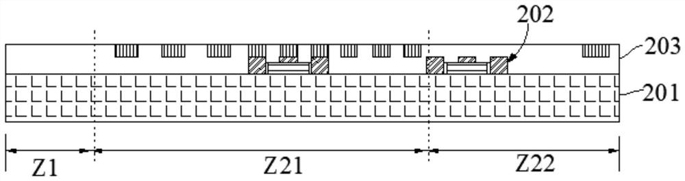
[0197] See Figure 16 In the present embodiment, the peripheral circuit chip includes a semiconductor substrate 201 and an peripheral circuit and an interconnect layer 203 in the semiconductor substrate 201, and the peripheral circuit and the interconnect layer 203 are further included. The peripheral circuit and peripheral interconnection layer formed on the semiconductor substrate 201; the peripheral circuit chip includes an internal region (including the core array region Z22 and step area Z21, which will be described later) and an edge region Z1 surrounding the internal region Z...


PUM


Abstract

The invention provides a three-dimensional memory and a preparation method thereof, and the three-dimensional memory comprises a peripheral circuit chip which comprises a semiconductor substrate, a peripheral circuit and an interconnection layer, wherein the peripheral circuit and the interconnection layer are sequentially formed on the semiconductor substrate, and a trench exposing the semiconductor substrate is formed in the edge region of the peripheral circuit chip; a bottom semiconductor layer, a middle semiconductor layer and a top semiconductor layer which are sequentially arranged on the groove, the peripheral circuit and the interconnection layer, wherein the middle semiconductor layer is composed of a middle layer main body part arranged in the internal area and a middle layer connecting part arranged in the first groove; in the trench, the bottom semiconductor layer, the intermediate semiconductor layer, and the top semiconductor layer are electrically connected to the semiconductor substrate. The trench is formed in the edge area of the peripheral circuit chip, the bottom semiconductor layer, the semiconductor sacrificial layer and the top semiconductor layer are electrically connected with the semiconductor substrate through the groove, and charged plasma generated in the array etching process can be guided away through the semiconductor substrate.

Description

Technical field [0001] The present invention belongs to the semiconductor design and manufacturing, and in particular, the present invention relates to a three-dimensional memory and a preparation method thereof. Background technique [0002] As the 3D memory (3D NAND) integration is getting higher and higher, the three-dimensional memory has evolved from 32 layers to 64 floors, even higher layer layers, and silicon nitride as the number of layers of the three-dimensional memory increases, silicon nitride And the number of tier sin & ox film increases, the etching depth of the step, the channel hole, the gate line, and the contact hole will increase, and there will be a lot of plasma (Plasma), etching during the etching process. The plasma generated during the process needs to be conducted by substrate; there is also a lot of charged plasma, etching during the etching process of the metal and the etching of Metal & Via in the back channel. The plasma generated in the process also...

Claims


Application Information

Patent Timeline
IPC IPC(8): H01L27/11565H01L27/1157H01L27/11573H01L27/11582
CPCH10B43/10H10B43/35H10B43/40H10B43/27Y02D10/00
Inventor 张坤吴林春周文犀
Owner YANGTZE MEMORY TECH CO LTD
Why Eureka
Try Eureka