Light-emitting diode epitaxial wafer and manufacturing method thereof

A technology for light-emitting diodes and a manufacturing method, which is applied to semiconductor devices, electrical components, circuits, etc., can solve the problems of effective recombination of carriers, low internal quantum luminous efficiency of light-emitting diodes, poor carrier confinement ability, etc. Effect of Internal Quantum Luminescence Efficiency

Active Publication Date: 2022-05-13
HC SEMITEK SUZHOU
View PDF3 Cites 0 Cited by
  • Summary
  • Abstract
  • Description
  • Claims
  • Application Information

AI Technical Summary

Problems solved by technology

[0004] However, the single-layer AlGaN quantum barrier layer has poor carrier confinement capabilities, which will cause carriers to fail to recombine effectively in the quantum well layer, which in turn will lead to low internal quantum luminescence efficiency of light-emitting diodes.

Method used


Image

  • Light-emitting diode epitaxial wafer and manufacturing method thereof
  • Light-emitting diode epitaxial wafer and manufacturing method thereof
  • Light-emitting diode epitaxial wafer and manufacturing method thereof

Examples


Embodiment Construction

[0028] In order to make the purpose, technical solution and advantages of the present disclosure clearer, the implementation manners of the present disclosure will be further described in detail below in conjunction with the accompanying drawings.

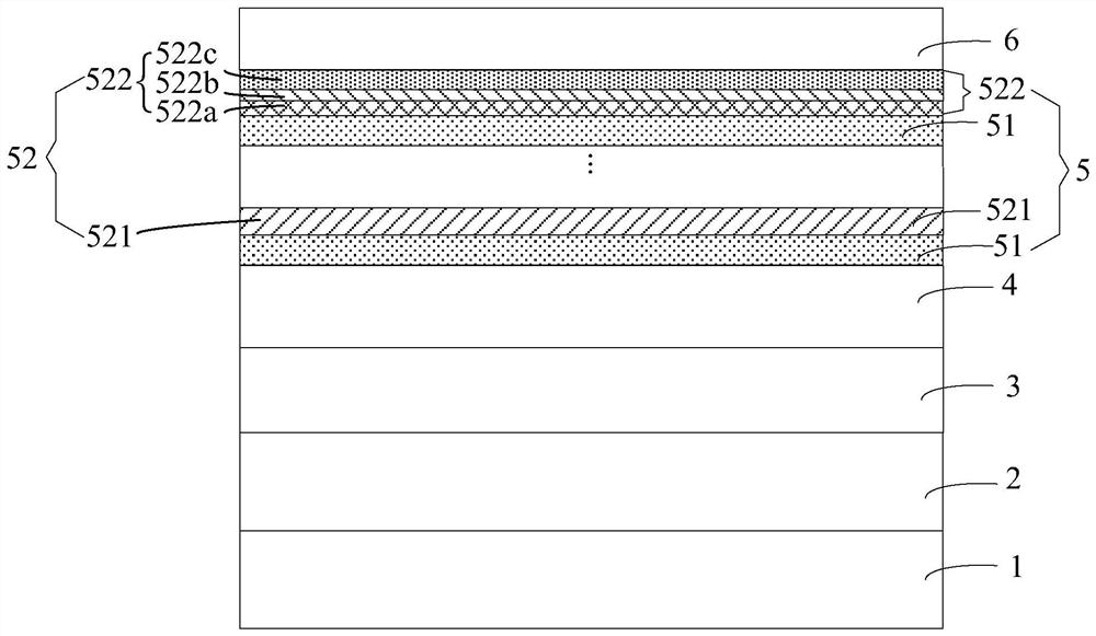
[0029] figure 1 is a schematic structural view of a light-emitting diode epitaxial wafer provided by an embodiment of the present disclosure, as shown in figure 1 As shown, the LED epitaxial wafer includes a substrate 1 , and a buffer layer 2 , an undoped AlGaN layer 3 , an N-type layer 4 , an active layer 5 and a P-type layer 6 stacked on the substrate 1 in sequence.

[0030] The active layer 5 includes a plurality of quantum well layers 51 and quantum barrier layers 52 alternately grown periodically, and each quantum well layer 51 is made of Al z Ga 1-z N layers. The multiple quantum barrier layers 52 include multiple first-type quantum barrier layers 521 close to the N-type layer 4 and multiple second-type quantum barrier lay...


PUM

PropertyMeasurementUnit
thicknessaaaaaaaaaa
thicknessaaaaaaaaaa
thicknessaaaaaaaaaa

Abstract

The disclosure provides a light-emitting diode epitaxial wafer and a manufacturing method thereof, which belong to the technical field of semiconductors. The active layer of the light-emitting diode epitaxial wafer includes a plurality of alternately grown quantum well layers and quantum barrier layers, and each quantum well layer is made of Al z Ga 1‑z N layer, the multiple quantum barrier layers include multiple first-type quantum barrier layers close to the N-type layer and multiple second-type quantum barrier layers close to the P-type layer, the first type of quantum barrier layer is Al m Ga 1‑m N layer, z<m, the second type of quantum barrier layer includes the first sublayer, the second sublayer and the third sublayer stacked in sequence, the first sublayer is Al x Ga 1‑x N layer, the second sublayer is Al y Ga 1‑y N layer, z<x<y, and the third sublayer is an AlN layer. The use of the light-emitting diode epitaxial wafer can improve the carrier confinement ability of the quantum barrier layer, so that more carriers can recombine in the quantum well layer, thereby improving the internal quantum luminous efficiency of the light-emitting diode.

Description

technical field [0001] The disclosure relates to the technical field of semiconductors, in particular to a light-emitting diode epitaxial wafer and a manufacturing method thereof. Background technique [0002] Short-wavelength light-emitting diodes based on AlGaN materials have a wide range of applications and are an important research content in the field of nitride semiconductor research. [0003] Epitaxial wafers are an important component in the manufacture of light-emitting diodes. The existing light-emitting diode epitaxial wafer includes a substrate, a buffer layer, an undoped AlGaN layer, an N-type layer, an active layer and a P-type layer stacked on the substrate in sequence. The active layer includes a plurality of alternately grown quantum well layers and quantum barrier layers, wherein the quantum barrier layer is usually an AlGaN layer with a single-layer structure. [0004] However, the single-layer AlGaN quantum barrier layer has a poor confinement ability t...

Claims


Application Information

Patent Timeline
Patent Type & Authority Patents(China)
IPC IPC(8): H01L33/06H01L33/32H01L33/00
CPCH01L33/06H01L33/32H01L33/325H01L33/007
Inventor 乔楠李昱桦刘源
Owner HC SEMITEK SUZHOU
Why Eureka
Try Eureka