Probe and test device

A technology of probes and test sockets, which is applied in the direction of measuring devices, measuring electricity, and measuring electrical variables, etc. It can solve problems such as increasing production costs, affecting the accuracy of information transmission, and unfavorable semiconductor testing, etc., to reduce impedance and shorten signal transmission paths Effect

Pending Publication Date: 2021-03-19
吴俊杰
View PDF0 Cites 2 Cited by
  • Summary
  • Abstract
  • Description
  • Claims
  • Application Information

AI Technical Summary

Problems solved by technology

[0006] However, since the upper contact piece 12, the lower contact piece 13 and the elastic component 14 move against the housing piece 11 during use, only the contact portion 123 of the upper contact piece 12 and the lower contact piece 13 The contact part 133 leans against the housing part 11 at the same time to form electrical conduction, the actual contact area between them is not large, and more contact points will increase the impedance during signal transmission, which is likely to generate noise during IC testing. Misjudgment is not conducive to semiconductor testing, not only the signal transmission speed cannot be effectively improved, but also the particles scraped off due to the mutual friction of the component surfaces are deposited in the housing part 11, affecting the correctness of information transmission
[0007] Furthermore, because the upper contact 12 and the lower contact 13 are designed in a pointed form, they will scratch the contact points when they contact the test contact A and the receiving contact B, which is commonly known as a scraper, which is not only harmful to the test equipment and The loss of parts is large, which is not conducive to the industrial mass production of the test process, and will also increase the production cost

Method used


Image

  • Probe and test device
  • Probe and test device
  • Probe and test device

Examples


Embodiment Construction

[0026] The features and technical contents of the relevant patent applications of the present invention will be clearly presented in the following detailed description of preferred embodiments with reference to the drawings. Before going into detail, it should be noted that like components are numbered the same.

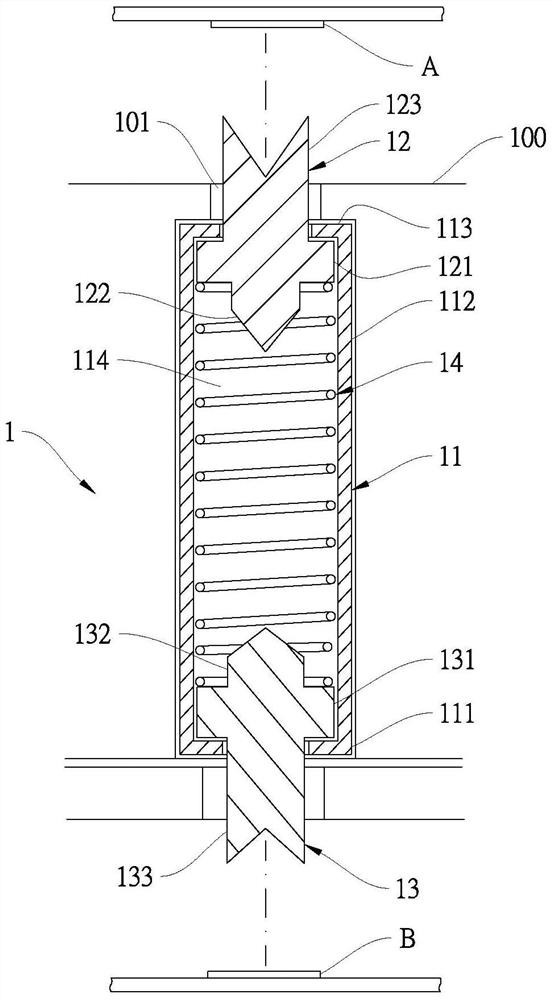
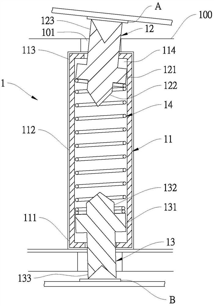
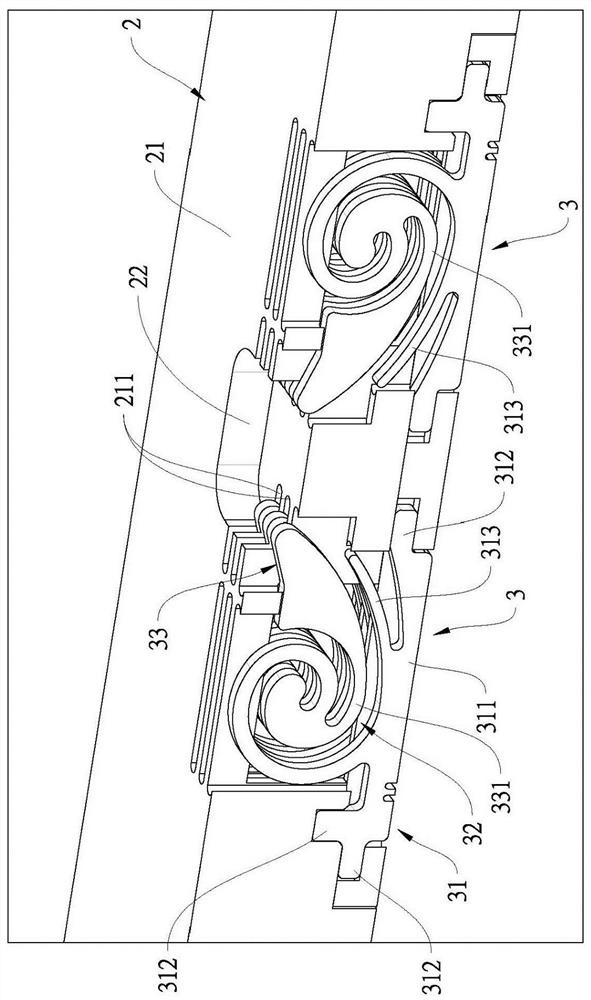
[0027] refer to image 3 Shown, be the preferred embodiment of testing device of the present invention, in order to test a chip 4 (shown in Figure 5 Middle), the test device includes a test seat 2, and several probes 3 arranged in the test seat 2 at intervals.

[0028] The test base 2 includes a base body 21 and a test space 22 formed on the base body 21 . Wherein, the seat body 21 has several installation holes 211 arranged at intervals. In this embodiment, the test space 22 is rectangular, and the several installation holes 211 are spaced along two sides of the test space 22. arrangement. It should be noted that the arrangement of the mounting holes 211 is des...


PUM


Abstract

The invention discloses a probe and a test device, which are used for testing a chip, the probe is arranged in a mounting hole of a test seat, the probe is in a sheet shape and is made of a conductivematerial, and the probe comprises a base part, a buffer part and a contact part, wherein the base part is located in the mounting hole and clamped on the test seat, the buffer part is located in themounting hole and integrally and spirally extends outwards from the base part, and the contact part is located in the mounting hole and integrally extends from the buffer part to be separated from thebase part; a tail end of the contact part protrudes out of the mounting hole and extends into the test space. The probe is integrally formed, so impedance and noise can be reduced, manufacturing costof the testing device comprising the probe is reduced, and assembling convenience is improved.

Description

technical field [0001] The invention relates to a testing device, in particular to a probe and a testing device for testing semiconductor components. Background technique [0002] With the advancement of semiconductor technology, the requirements for the precision of testing equipment have been greatly increased. In the case of IC testing or high-frequency testing, the test signal is transmitted by the probe, so when the probe that conducts the signal has many contact points , It is easy to produce discontinuous surface and form impedance discontinuity, which will cause the reflection loss and distortion of the test signal, and too many contact points will also make the response speed of the probe slower, which will affect the accuracy of the test. [0003] refer to figure 1 As shown, the conventional test probe 1 is replaceably disposed in a probe hole 101 of a test socket 100 for electrically connecting a test contact A and a receiving contact B. As shown in FIG. The tes...

Claims


Application Information

Patent Timeline
Patent Type & Authority Applications(China)
IPC IPC(8): G01R1/073
CPCG01R1/07357
Inventor 吴俊杰
Owner 吴俊杰
Why Eureka
Try Eureka