Middle frame of electronic product and manufacturing method thereof, casing of electronic product and electronic product

A technology for electronic products and production methods, which is applied to electrical equipment shells/cabinets/drawers, electrical components, chassis/boxes/drawer parts, etc., can solve the problem of low color brightness, no ceramic white color effect, and inability to achieve Ceramic white and other problems, to achieve high brightness, brilliant effect, and improve the effect of overall brightness

Active Publication Date: 2022-06-21
SHENZHEN YUNMI C CRPTOLOG COMM TECH CO LTD
View PDF16 Cites 0 Cited by
  • Summary
  • Abstract
  • Description
  • Claims
  • Application Information

AI Technical Summary

Problems solved by technology

However, due to the use of a mixture of various substances, the spray paint has only whiteness in the chroma of the color, but does not have the color effect of ceramic white, and the brightness of the color is low, so it cannot achieve the effect of ceramic white.
However, the method of coating can only achieve metallic silver white and bright gray

Method used


Image

  • Middle frame of electronic product and manufacturing method thereof, casing of electronic product and electronic product
  • Middle frame of electronic product and manufacturing method thereof, casing of electronic product and electronic product
  • Middle frame of electronic product and manufacturing method thereof, casing of electronic product and electronic product

Examples


preparation example Construction

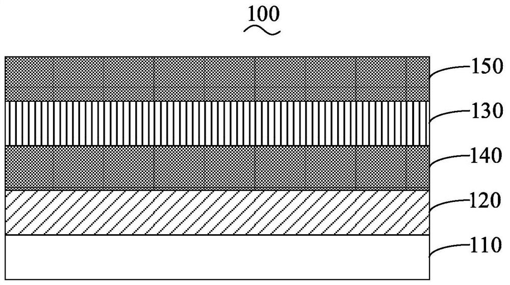
[0052] The preparation process of the first UV adhesive layer 140 includes: the pre-baking temperature is 50°C-60°C, the pre-baking time is 3min-5min; the humidity of the spray booth is 45%-70%, and the temperature of the spray booth is 18-25°C; UV The irradiation energy of the furnace is 900mj / cm 2 ~1200mj / cm 2 . The above only lists a preparation process of a commonly used UV glue layer, but is not limited to this, and can also be a preparation process of a UV glue layer commonly used in the art.

[0053] Further, the thickness of the first UV adhesive layer 140 is 8 μm˜12 μm. In one embodiment, the thickness of the first UV adhesive layer 140 is 8 μm, 9 μm, 10 μm, 11 μm or 12 μm.

[0054] The function of the second UV adhesive layer 150 is mainly to protect the optical film layer 130 and at the same time improve the overall wear resistance of the middle frame 100 of the electronic product. The composition and preparation process of the second UV adhesive layer 150 are t...

Embodiment 1

[0091] The manufacturing process of the middle frame of the electronic product of the present embodiment is as follows:

[0092] (1) A coating layer with a thickness of 15 μm is formed by spraying on the substrate. Wherein, the raw material of the coating layer is composed of a coating main agent with a mass ratio of 1:3 and 783 slow-drying water (thinner). In parts by mass, the coating main agent is composed of 20 parts of ABS resin, 30 parts of titanium dioxide (white pigment), 30 parts of 783 slow-drying water (solvent) and 2 parts of dispersant (auxiliary).

[0093] (2) A first UV adhesive layer with a thickness of 10 μm is formed on the side of the coating layer away from the substrate. The raw material of the first UV adhesive layer is composed of photoinitiator, auxiliary agent and 783 slow drying water (diluent).

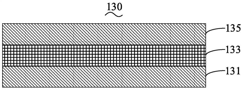
[0094] (3) forming a first high refractive index layer, a first low refractive index layer and a second high refractive index layer by sputtering in seque...

Embodiment 2

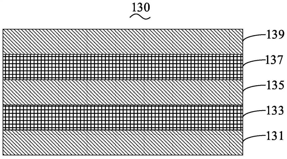
[0097] The manufacturing process of the middle frame of the electronic product of Example 2 is similar to the manufacturing process of the middle frame of the electronic product of Example 1, except that the material and thickness of the optical thin film layer are different. In the optical thin film layer of Example 2, the material of the first high refractive index layer is TiO 2 , the thickness is 21nm, the material of the first low refractive index layer is SiO 2 , with a thickness of 28 nm. The material of the second high refractive index layer is TiO 2 , with a thickness of 39 nm.


PUM

PropertyMeasurementUnit
thicknessaaaaaaaaaa
thicknessaaaaaaaaaa
thicknessaaaaaaaaaa

Abstract

The invention relates to a middle frame of an electronic product and a manufacturing method thereof, a casing of the electronic product and the electronic product. The middle frame of the above-mentioned electronic product includes a substrate, a paint layer arranged on the substrate, and an optical film layer arranged on the side of the paint layer away from the substrate. The raw materials for preparing the paint layer include paint main agents and diluents, in parts by mass In total, the paint main agent includes: 15-35 parts of resin, 20-40 parts of white pigment, 25-45 parts of solvent and 1-6 parts of additives. The optical film layer includes at least one high refractive index layer and at least one The low refractive index layer, the high refractive index layer and the low refractive index layer are arranged alternately, and the outermost layer of the optical film layer away from the substrate is a high refractive index layer. The Lab color index of the middle frame of the electronic product is: L=50 ~60, a=-5~0, b=0~5. The middle frame of the above-mentioned electronic product has a ceramic white appearance and high brightness.

Description

technical field [0001] The invention relates to the field of electronic products, in particular to a middle frame of an electronic product and a manufacturing method thereof, a casing of the electronic product and an electronic product. Background technique [0002] In the current decorative colors, ceramic white has always occupied a relatively large proportion, especially in electronic products, people prefer the appearance of white, and the proportion of white appearance accounts for almost half. In general electronic products, the shell materials are generally made of plastic and metal, and spraying and oxidation are usually used to improve the appearance. However, if plastic is used for electronic products such as mobile phones, it cannot meet customer requirements in terms of performance and appearance. Most of them are glass, composite panels, ceramics and other materials. These materials have good mechanical properties, and the appearance color is achieved by silk sc...

Claims


Application Information

Patent Timeline
Patent Type & Authority Patents(China)
IPC IPC(8): H05K5/02C09D155/02C09D7/61C09D7/20
CPCH05K5/0243C09D155/02C09D7/61C09D7/20C08K2003/2241C08K3/22
Inventor 张春姣周天济
Owner SHENZHEN YUNMI C CRPTOLOG COMM TECH CO LTD
Why Eureka
Try Eureka