Array substrate and display panel

A technology for array substrates and display panels, which is applied in the fields of instruments, optics, nonlinear optics, etc., can solve the problems of hindering the conduction of the driving circuit, insulating the driving circuit, increasing the risk of PI liquid diffusion and overflowing the driving circuit, etc., to achieve increased The effect of the blank area, reducing the footprint, and reducing the risk of preventing the conduction of the drive circuit

Active Publication Date: 2022-07-12
WUHAN CHINA STAR OPTOELECTRONICS TECH CO LTD
View PDF6 Cites 0 Cited by
  • Summary
  • Abstract
  • Description
  • Claims
  • Application Information

AI Technical Summary

Problems solved by technology

In the process of coating PI liquid, the PI liquid should not overflow the driving circuit (otherwise it will cause the insulation of the driving circuit and hinder the conduction of the driving circuit), which will increase the difficulty of coating the PI liquid
The current design method of the area where the driving circuit is located is: forming the driving circuit in the entire large groove, so that the probability of the PI liquid spreading and overflowing the large groove increases, thereby causing the PI liquid to diffuse and overflowing the driving circuit. increased risk

Method used


Image

  • Array substrate and display panel
  • Array substrate and display panel
  • Array substrate and display panel

Examples


Embodiment Construction

[0026] The technical solutions in the embodiments of the present application will be clearly and completely described below with reference to the accompanying drawings in the embodiments of the present application. Obviously, the described embodiments are only a part of the embodiments of the present application, but not all of the embodiments. Based on the embodiments in this application, all other embodiments obtained by those skilled in the art without creative efforts shall fall within the protection scope of this application.

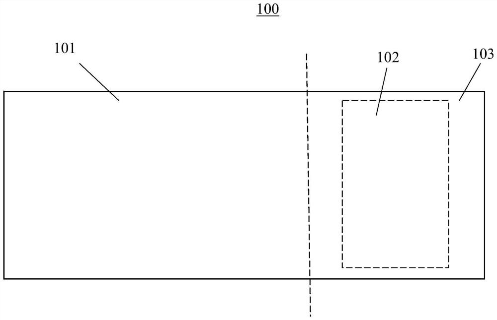
[0027] In the description of the application, it should be understood that the orientation or positional relationship indicated by the terms "width", "upper", "lower", etc. is based on the orientation or positional relationship shown in the accompanying drawings, and is only for the convenience of describing the application and to simplify the description, rather than to indicate or imply that the device or element referred to must have a particula...


PUM


Abstract

The present application provides an array substrate. The array substrate includes a display area and a non-display area surrounding the display area; the non-display area further includes a binding area; At least two diversion grooves and at least two groups of driving circuit holes are formed on the array substrate, one of the diversion grooves surrounds a group of the driving circuit holes; each of the diversion grooves includes a a first inner wall, the first inner wall is far away from the corresponding driving circuit hole, the first inner wall includes at least one arc-shaped segment facing the display area and at least one connecting segment smoothly connecting the arc-shaped segment . The present application also provides a display panel. The array substrate and the display panel provided by the present application can reduce the risk of the alignment film forming liquid flowing through the diversion groove and reduce the coating difficulty of the alignment film forming liquid.

Description

technical field [0001] The present application relates to the field of display technology, and in particular, to an array substrate and a display panel. Background technique [0002] In Thin Film Transistor-Liquid Crystal Display (TFT-LCD), a Chip On Film (COF) substrate is usually used to connect a Printed Circuit Board (PCB) and an array substrate together. Thereby, the PCB board can output the driving control signal to the array panel to complete the corresponding driving control. One end of the COF substrate is electrically connected to the driving circuit of the array substrate, and the other end is electrically connected to the PCB board. In the current liquid crystal display panel, an alignment film is provided on the side of the array substrate. The alignment film can provide a pre-tilt angle to the liquid crystal molecules, so that the liquid crystal molecules are arranged in an orderly manner. For the formation of the alignment film, an alignment film forming li...

Claims


Application Information

Patent Timeline
Patent Type & Authority Patents(China)
IPC IPC(8): G02F1/1333G02F1/1345G02F1/1337
CPCG02F1/1333G02F1/13452G02F1/1337G02F1/133723
Inventor 吴云飞
Owner WUHAN CHINA STAR OPTOELECTRONICS TECH CO LTD
Why Eureka
Try Eureka