Digital signal time delay method based on FPGA and high-precision time delay chip

A digital signal and delay chip technology, applied in the field of electronics, can solve the problems of not being able to reach large-scale physics, and the resolution is only at the nanosecond level, and achieve the effect of simple and reliable hardware circuits, improving delay resolution, and reducing errors

Pending Publication Date: 2021-03-26
INST OF NUCLEAR PHYSICS & CHEM CHINA ACADEMY OF
View PDF0 Cites 0 Cited by
  • Summary
  • Abstract
  • Description
  • Claims
  • Application Information

AI Technical Summary

Problems solved by technology

Therefore, although the delay resolution of this method can reach 10 ps level, its delay dynamic range is only a few microseconds, which cannot meet the requirements of large-scale physical experiments;
[0005] The second type is to use a field programmable logic gate array (FPGA) chip to build a coarse counter to realize the delay. This method has a large dynamic range of delay and can meet the experimental requirements, but because the resolution of the delay is determined by the rough counter Determined by the clock cycle, the clock cycle is often nanoseconds, so the resolution of this method is only nanoseconds

Method used


Image

  • Digital signal time delay method based on FPGA and high-precision time delay chip
  • Digital signal time delay method based on FPGA and high-precision time delay chip
  • Digital signal time delay method based on FPGA and high-precision time delay chip

Examples


Embodiment 1

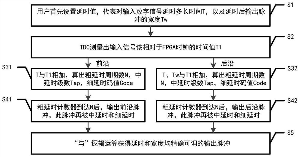
[0028] In this embodiment, a digital signal delay method of coarse delay+medium delay+fine delay is improved, such as image 3 The illustrated embodiment includes the following steps:

[0029] S1: The user sets the delay time T of the input signal and the width Tw of the output pulse after the delay according to the requirements; the parameters T and Tw satisfy the following relationship: Tn -1), T+Twn -1), wherein, n is the number of digits of the coarse counter, and Tclk is the coarse delay clock cycle, and it is not difficult to find out that the maximum value setting of T and Tw is related to the setting of the number of digits of the coarse counter by the above formula;

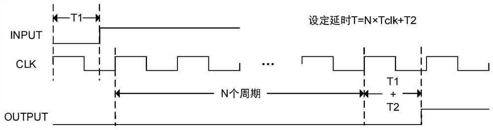
[0030] S2: Use TDC to measure the time value T1 of the input signal relative to the FPGA clock, such as Figure 4 As shown, the present embodiment obtains the time value of the input signal relative to the FPGA clock by the TDC built in the FPGA, in addition, it can also be measured with a dedicated TDC ...


PUM


Abstract

The invention discloses a digital signal delay method based on an FPGA (Field Programmable Gate Array) and a high-precision delay chip. The method comprises the following steps: firstly, calculating adelay parameter of a front edge or a rear edge of a digital signal by utilizing a delay duration T set by a user, a width Tw of a delayed output pulse and a measured time value T1 of an input signalrelative to an FPGA clock; carrying out delay processing on the digital signal by using the delay parameter; and finally, synthesizing the front edge and the rear edge of the signal subjected to timedelay processing through logical operation to obtain an output pulse with accurate and adjustable time delay and width. According to the digital signal time delay method, the FPGA and the high-precision time delay chip are utilized, the digital signal time delay mode of combining coarse time delay with medium time delay and fine time delay is adopted, signal time delay jitter is effectively reduced, the time delay resolution is improved, most functions of the method are completed in one chip, a hardware circuit is simple and reliable, the integration degree is high, and the delay error is effectively reduced.

Description

technical field [0001] The invention belongs to the technical field of electronics, and in particular relates to a digital signal delay method based on an FPGA and a high-precision delay chip. Background technique [0002] In modern large-scale physical experiments, electronic equipment and instruments generally use electric pulse trigger signals to start and stop, or use pulse trigger signals to trigger a certain function of the test equipment in the test. figure 1 It is a schematic diagram of the device structure of an existing typical large-scale physical experiment. It can be seen from the figure that the positions of each equipment or instrument are different. The requirements for the time and width of the electrical pulse trigger signal input to the device or instrument are also different. In some experiments with higher requirements, the equipment and instruments not only require the time and width resolution of the trigger signal to reach 10 ps level, but also have ...

Claims


Application Information

Patent Timeline
IPC IPC(8): G05B19/042
CPCG05B19/0423G05B2219/23216
Inventor 刘金鑫吴军袁晨叶岑明杜亚飞杨波
Owner INST OF NUCLEAR PHYSICS & CHEM CHINA ACADEMY OF
Why Eureka
Try Eureka