Check patentability & draft patents in minutes with Patsnap Eureka AI!

Novel CMOS image sensor pixel structure

An image sensor and pixel structure technology, applied in the field of CMOS image sensor pixel structure, can solve the problems of image smear, increase the area of ​​photodiode photosensitive area, etc., and achieve the effect of increasing the area and improving the image quality.

Pending Publication Date: 2021-04-06
GPIXEL
View PDF11 Cites 0 Cited by
  • Summary
  • Abstract
  • Description
  • Claims
  • Application Information

AI Technical Summary

Problems solved by technology

[0005] The present invention aims to solve the problem of image smear caused by directly increasing the area of ​​the photosensitive region of the traditional CMOS image sensor, and provides a new CMOS image sensor pixel structure, which can increase the photoelectricity without affecting the charge transfer speed of the transfer transistor. The area of ​​the photosensitive region of the diode

Method used


Image

  • Novel CMOS image sensor pixel structure
  • Novel CMOS image sensor pixel structure
  • Novel CMOS image sensor pixel structure

Examples


Embodiment Construction

[0018] In order to make the object, technical solution and advantages of the present invention clearer, the present invention will be further described in detail below in conjunction with the accompanying drawings and specific embodiments. It should be understood that the specific embodiments described here are only used to explain the present invention, but not to limit the present invention.

[0019] The pixel structure of the novel CMOS image sensor provided by the embodiments of the present invention will be described in detail below.

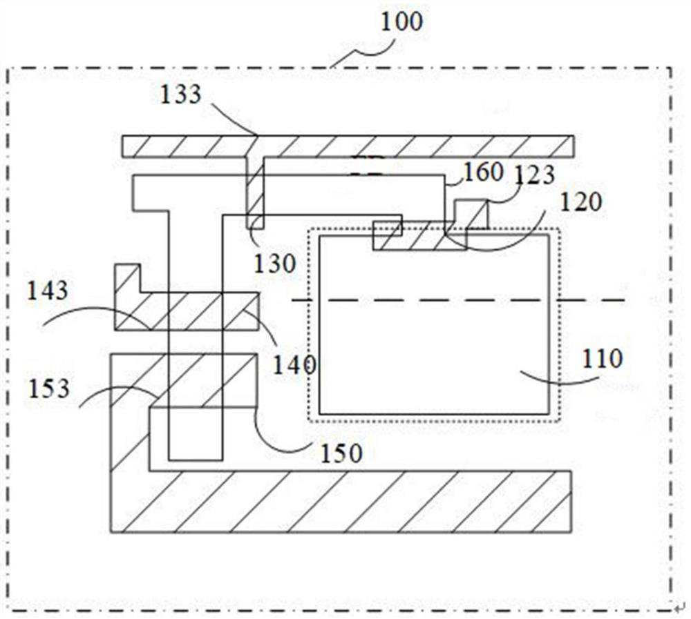
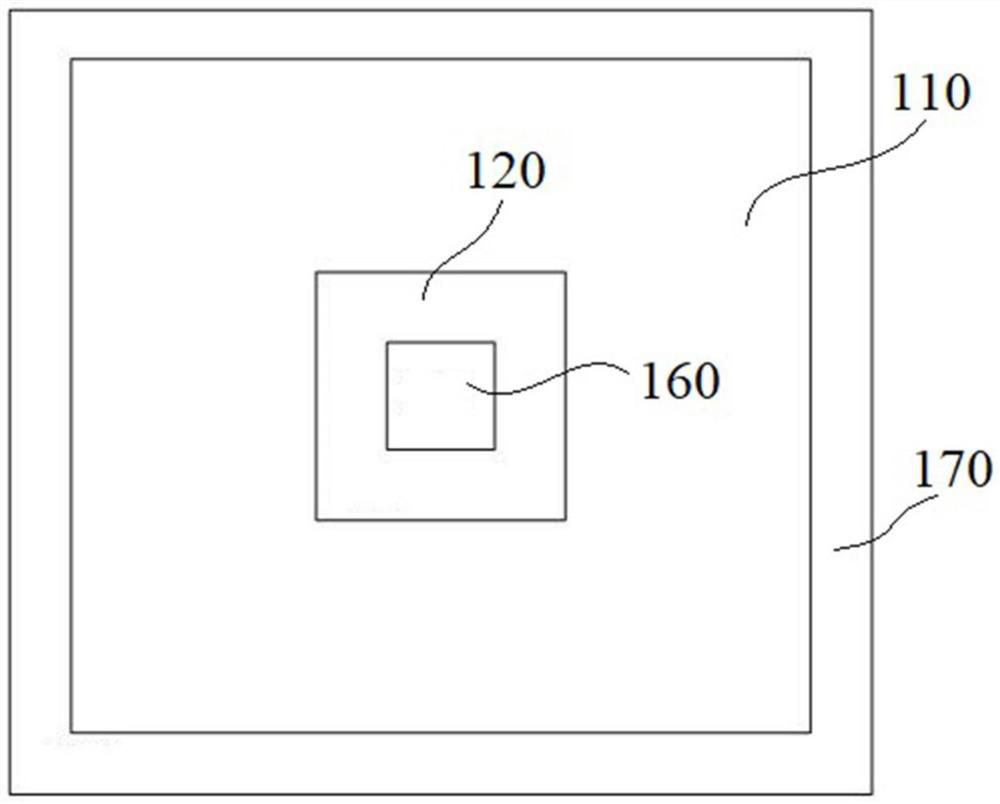
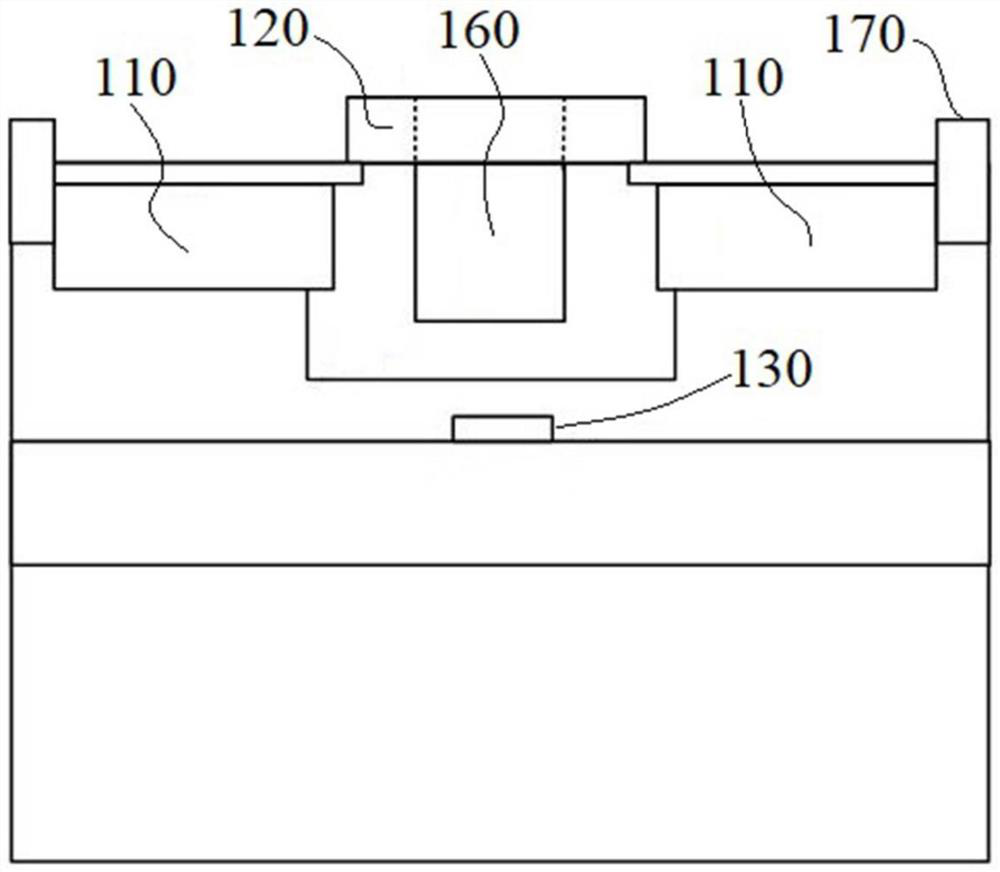
[0020] like figure 2 and image 3 As shown, the novel CMOS image sensor pixel structure provided by the present invention includes a photodiode 110, a transfer transistor 120, a reset transistor 130, and a floating diffusion node 160; The node 160 is arranged in the hollow area of ​​the photodiode 110, the transfer transistor 120 has a ring structure, its inner edge is in contact with the floating diffusion node 160, and its outer edge i...


PUM


Abstract

The invention provides a novel CMOS image sensor pixel structure. The novel CMOS image sensor pixel structure comprises a photodiode, a floating diffusion node, a reset transistor and a transfer transistor, wherein the photodiode is of a hollow annular structure, the floating diffusion node is arranged in a hollow area of the photodiode, the transfer transistor is of an annular structure, the inner edge of the transfer transistor is in contact with the floating diffusion node, the outer edge of the transfer transistor is in contact with the photodiode, and the reset transistor is arranged under the floating diffusion node. Charges accumulated by the photodiode are transferred from different directions to the floating diffusion node through the transfer transistor, a vertical electric field is provided through the reset transistor, and the floating diffusion node is reset. The area of the photosensitive region of the photodiode can be increased under the condition that the charge transfer speed of the transfer transistor is not influenced.

Description

technical field [0001] The invention relates to the technical field of CMOS image sensors, in particular to a CMOS image sensor pixel structure based on a ring photosensitive element. Background technique [0002] CMOS image sensors are becoming more and more popular in scientific and commercial applications due to their low power consumption, low cost and high integration capability. With the continuous expansion of the application range of CMOS image sensors, people have higher requirements for their performance, and they are constantly developing towards higher resolution, wider dynamic range, and faster speed. Generally, for an image sensor with the same resolution, the larger the photosensitive area, the better the imaging quality. For the optical format attribute of the camera, the imaging quality of 2 / 3" is better than that of 1 / 2" in most conditions, especially in low-light environments. Therefore, how to increase the area of ​​the photosensitive unit of the image ...

Claims


Application Information

Patent Timeline
IPC IPC(8): H01L27/146H04N5/374
CPCH01L27/14603H01L27/14607H01L27/1461H01L27/14612H01L27/14643H04N25/76
Inventor 王欣洋李扬马成刘洋辛国松
Owner GPIXEL
Features
  • R&D
  • Intellectual Property
  • Life Sciences
  • Materials
  • Tech Scout
  • Unparalleled Data Quality
  • Higher Quality Content
  • 60% Fewer Hallucinations
Learn More