
Method for improving 850nm semiconductor laser power density

A laser power and semiconductor technology, which is applied in the direction of semiconductor lasers, semiconductor laser devices, semiconductor laser optical devices, etc., can solve the problems of high-power semiconductor lasers with large light divergence angles and poor light quality.

Pending Publication Date: 2021-04-09
HAINAN NORMAL UNIV
View PDF0 Cites 0 Cited by
  • Summary
  • Abstract
  • Description
  • Claims
  • Application Information

AI Technical Summary

Problems solved by technology

High-power semiconductor lasers cannot be directly used in industrial processing and military fields due to their shortcomings such as large light divergence angle, elliptical Gaussian beam and poor light quality.

Method used


Image

  • Method for improving 850nm semiconductor laser power density
  • Method for improving 850nm semiconductor laser power density

Examples


Embodiment Construction

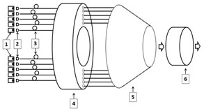
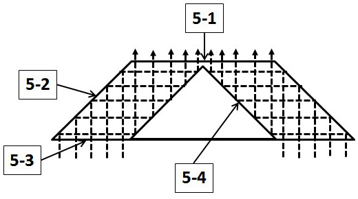
[0014] Combine below figure 1 and figure 2 The present invention is further described in detail.

[0015] The invention discloses a method for increasing the power density of an 850nm semiconductor laser, which includes an 850nm semiconductor laser single-tube module (1), a collimating mirror (2), an optical fiber (3), a ring holder (4), and a hollow trapezoidal round table ( 5) and focusing mirror (6). The hollow trapezoidal round platform (5) comprises the upper bottom surface of the round platform (5-1), the outer side of the round platform (5-2), the lower bottom surface of the round platform (5-3) and the inner side of the round platform (5-4).

[0016] figure 1 Take ten 850nm semiconductor laser single-tube modules in a single direction as an example for specific description. Each 850nm semiconductor laser single-tube module of ten 850nm semiconductor laser single-tube modules (1) is coupled into an optical fiber (3) through a collimator (2), and the optical fiber (...


PUM


Abstract

The invention discloses a method for improving 850nm semiconductor laser power density. According to the method, a 850nm semiconductor laser single-tube module (1), collimating mirrors (2), optical fibers (3), an annular fixator (4), a hollow trapezoidal circular truncated cone (5) and a focusing mirror (6) are adopted. The hollow trapezoid circular truncated cone (5) comprises a circular truncated cone upper bottom face (5-1), a circular truncated cone outer side face (5-2), a circular truncated cone lower bottom face (5-3) and a circular truncated cone inner side face (5-4); the light of the 850nm semiconductor laser single-tube modules (1) is coupled into the optical fibers (3) through the collimating mirrors (2); the optical fibers (3) pass through the annular fixator (4) and then the light vertically enters the lower bottom face (5-3) of the hollow trapezoidal circular truncated cone (5), undergoes total reflection at the outer side face (5-2) and the inner side face (5-4) of the circular truncated cone and enters the focusing mirror (6); and therefore, 850nm semiconductor laser output can be improved.

Description

technical field [0001] The invention relates to the technical field of high-power semiconductor lasers, in particular to a method for increasing the power density of 850nm semiconductor lasers. Background technique [0002] High-power semiconductor lasers are widely used in industrial processing and military fields due to their small size, light weight, and high electro-optical conversion. High-power semiconductor lasers cannot be directly used in industrial processing and military fields due to their shortcomings such as large light divergence angle, elliptical Gaussian beam and poor light quality. In order to speed up the direct application of high-power semiconductor lasers in industrial processing and military fields, a method for increasing the power density of 850nm semiconductor lasers is proposed, which can effectively increase the output power density of 850nm semiconductor lasers. Contents of the invention [0003] The purpose of the invention is to propose a me...

Claims


Application Information

Patent Timeline
Patent Type & Authority Applications(China)
IPC IPC(8): H01S5/40H01S5/00
CPCH01S5/005H01S5/4012
Inventor 李再金袁毅杨云帆杨隆杰赵志斌陈浩李林乔忠良曾丽娜曲轶
Owner HAINAN NORMAL UNIV
Learn More