Laser light source module and projection display system

A laser light source and module technology, applied in optics, instruments, projection devices, etc., can solve the problems of large spot gap, large overall volume, and energy loss of laser light source, achieve high laser power density, small size, and avoid energy loss. Effect

Inactive Publication Date: 2020-02-18
深圳市TCL高新技术开发有限公司
View PDF6 Cites 0 Cited by
  • Summary
  • Abstract
  • Description
  • Claims
  • Application Information

AI Technical Summary

Problems solved by technology

[0005] The technical problem to be solved by the present invention is to provide a laser light source module and a projection display system for the above-mentioned defects of the prior art, aiming at solving the problem of large gaps between laser light spots, large overall volume and problems in the prior art. Reducing the laser output spot size requires two reflections, which is likely to cause problems such as high energy loss

Method used


Image

  • Laser light source module and projection display system
  • Laser light source module and projection display system
  • Laser light source module and projection display system

Examples


Embodiment 1

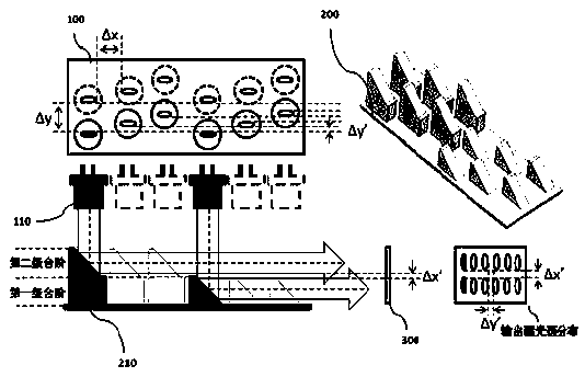
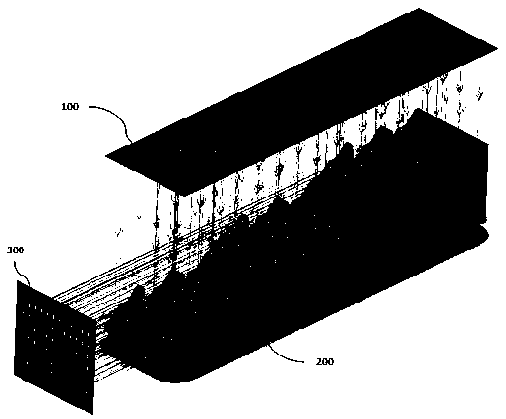
[0037] Such as figure 1 As shown in , in this embodiment, all semiconductor lasers are packaged on the same heat dissipation substrate, and the semiconductor laser arrays 100 are arranged in three groups, and every four semiconductor lasers 110 is a group. Since the collimating mirror does not have a directional cover for the laser beam emitted by the semiconductor laser 110 , the spot distribution after being collimated by the collimating mirror can be regarded as the distribution of the semiconductor laser 110 . Therefore from figure 1 It can be seen from the distribution of the elliptical spot after the semiconductor laser 110 is collimated by the collimating mirror (not shown in the figure) that figure 1 It can be seen that the row spacing Δx (the distance between two adjacent semiconductor lasers 110 ) and the column spacing Δy (the gap between two adjacent elliptical spots in the short axis direction) of the spots of the original laser light source are relatively large,...

Embodiment 2

[0043] Such as figure 2 As shown, in this embodiment, the semiconductor laser array 100 is arranged into 2 large groups, and each large group is divided into 3 small groups, and there are 2 semiconductor lasers 110 in each small group, so in this embodiment, there are 12 semiconductor laser arrays 100 . In the semiconductor laser array in this embodiment, the large groups are arranged sequentially along the long axis direction of the elliptical light spot after the semiconductor lasers are collimated by the collimating mirror, and there is no dislocation arrangement. And between the groups with a certain interval Δy , Misalignment settings, such as figure 2 shown in .

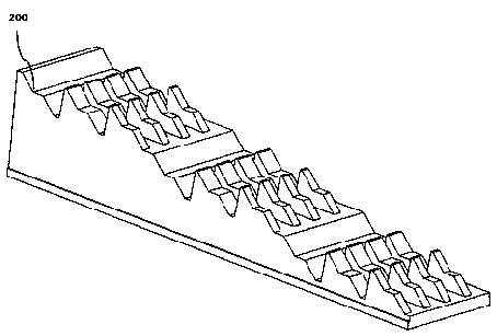
[0044] Correspondingly, the stepped reflector array 200 is also set into 2 groups, and each group is divided into 3 groups, with 12 stepped reflectors 210, and each stepped reflector 210 has only one step (reflecting surface ), so that the stepped reflector 210 corresponds to the semiconductor laser 110 o...

Embodiment 3

[0047] Such as Figure 3-5 As shown, in this embodiment, the semiconductor laser array 100 is arranged into 3 large groups, and each large group is divided into 3 small groups, and each group is provided with 8 semiconductor lasers 110, so in this embodiment, a total of Seventy-two semiconductor lasers 110 are provided. from Figure 5 It can be seen from the figure that in the semiconductor laser array 100 in this embodiment, the large groups are arranged sequentially along the long axis direction of the elliptical spot after the semiconductor laser is collimated by the collimating mirror, and there is no misalignment. And between the groups with a certain interval Δy , Misplaced settings.

[0048] Correspondingly, the stepped reflector array 200 in this embodiment is also provided with 3 large groups, and each large group is further divided into 3 subgroups, and each subgroup is provided with 4 stepped reflector arrays 210 . Since all the stepped reflectors 210 in this em...


PUM


Abstract

The invention discloses a laser light source module and a projection display system. The laser light source module comprises a semiconductor laser array packaged on a heat dissipation substrate; a stepped mirror array for reflecting the laser beam emitted by the semiconductor laser array; and an output surface arranged in the output direction of the reflected light. The semiconductor lasers in thesemiconductor laser array are staggered at preset intervals. The stepped mirrors in the stepped mirror array are corresponding to the semiconductor lasers and are staggered along the laser emitting direction of the semiconductor laser array so that the laser beam emitted by the semiconductor lasers is reflected by the corresponding stepped mirrors once and then outputs light spots to the output surface. The laser light source module only needs to perform one time of reflection so that the row spacing and the column spacing between the light beams can be reduced, the smaller volume can be ensured, the higher laser power density can be obtained and the energy loss caused by secondary mirror reflection and the technological complexity can be avoided.

Description

technical field [0001] The invention relates to the technical field of laser display, in particular to a laser light source module and a projection display system. Background technique [0002] In recent years, laser display technology has been widely used in various occasions due to its advantages of high brightness, wide color gamut, high color reproduction, long life, energy saving and environmental protection. In laser display technology, because semiconductor lasers have the advantages of high brightness, small size, long life, low cost and high reliability, semiconductor lasers are often used as laser light sources. However, due to the limitations of the semiconductor process level and the characteristics of the material itself, the current output optical power of a single semiconductor laser is low, mostly between several hundred milliwatts and several watts. In order to meet the needs of laser display products for high-power laser light sources, in practical applica...

Claims


Application Information

Patent Timeline
Patent Type & Authority Applications(China)
IPC IPC(8): G03B21/20
CPCG03B21/2033G03B21/2066
Inventor 杨兴许礼强王瑞
Owner 深圳市TCL高新技术开发有限公司
Why Eureka
Try Eureka