Array substrate, display panel and display device

A technology for array substrates and substrate substrates, applied in nonlinear optics, instruments, optics, etc., can solve problems such as limited aperture ratio, achieve the effects of reducing line width, improving display effect, and increasing light transmission area

Pending Publication Date: 2022-02-25
CHANGSHA HKC OPTOELECTRONICS CO LTD +1
View PDF3 Cites 2 Cited by
  • Summary
  • Abstract
  • Description
  • Claims
  • Application Information

AI Technical Summary

Problems solved by technology

[0002] In a liquid crystal display panel, the smallest repeating unit of an existing array substrate is a sub-pixel, and a sub-pixel usually includes a scanning line, a data line, a transistor, a common electrode, a pixel electrode, etc., and then the smallest repeating unit Array arrangement is carried out, but due to the requirements of the process on line width (CD) and line distance (spec), the light-emitting area is squeezed, that is, the aperture ratio is limited

Method used


Image

  • Array substrate, display panel and display device
  • Array substrate, display panel and display device
  • Array substrate, display panel and display device

Examples


Embodiment 1

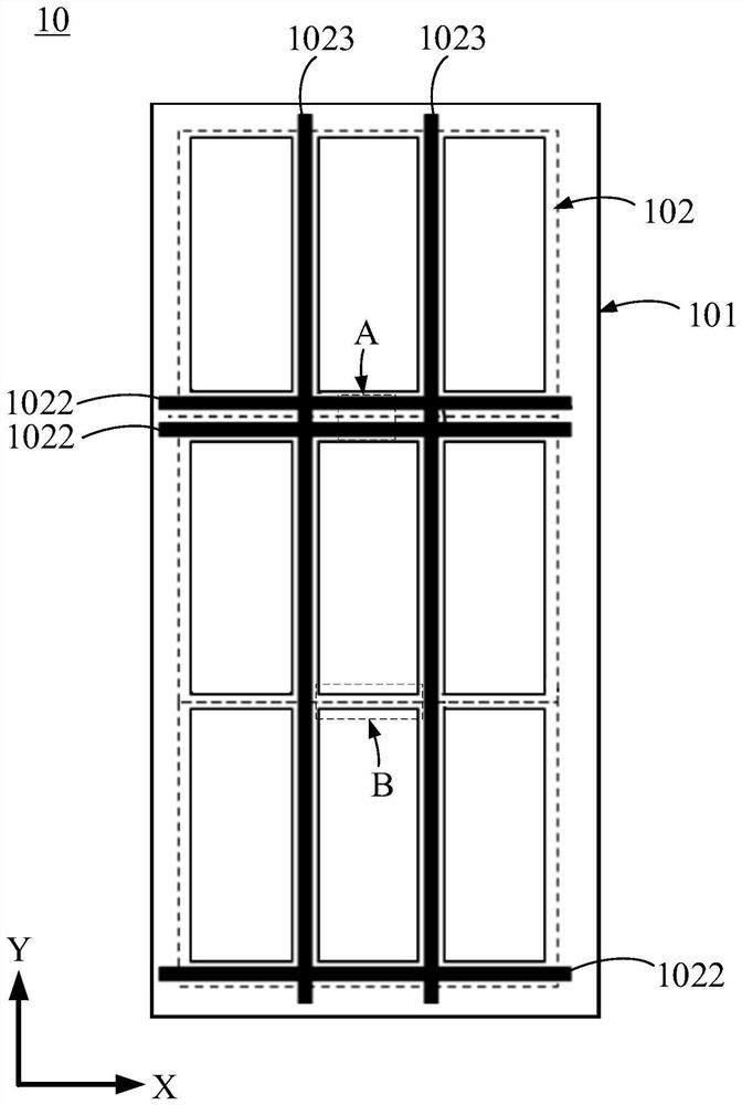
[0044] like figure 1 As shown, an embodiment of the present disclosure provides an array substrate 10 , and the array substrate 10 may include a base substrate 101 and a plurality of sub-pixels 102 .

[0045] The base substrate 101 may be a glass substrate, but not limited thereto, and may also be a substrate made of other materials, such as PI material and the like.

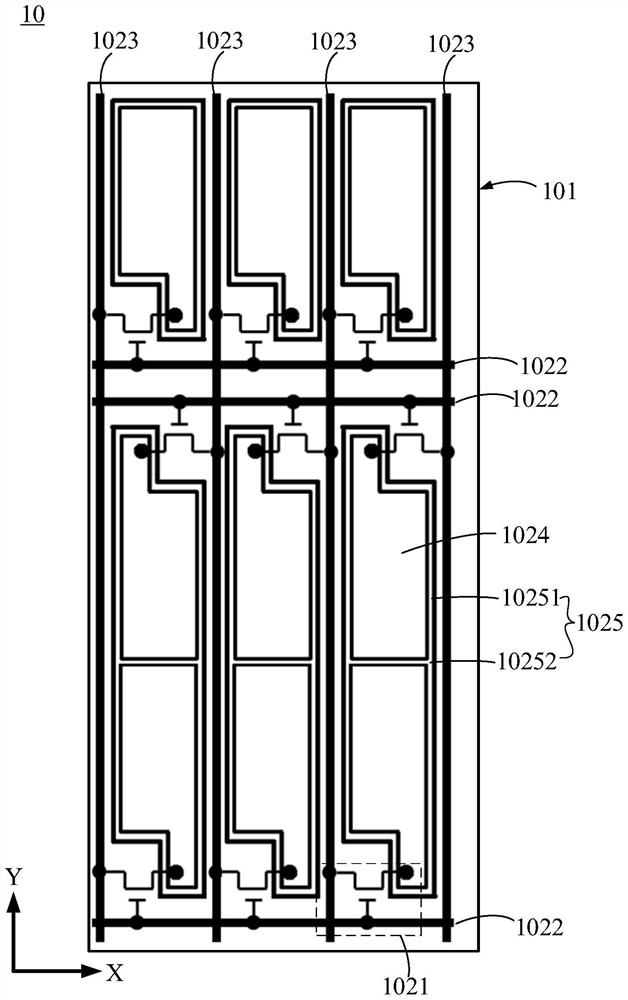
[0046] combine figure 1 and figure 2 As shown, a plurality of sub-pixels 102 may be arrayed on the base substrate 101 along the row direction X and the column direction Y, and the sub-pixels 102 may include transistors 1021 , pixel electrodes 1024 , common electrodes 1025 , data lines 1023 and scan lines 1022 .

[0047] Specifically, the transistor 1021 may include a gate electrode not shown in the figure, an active layer, and a first electrode and a second electrode disposed in the same layer, and a gate insulating layer may be provided between the gate electrode and the active layer, so that the gate The ...

Embodiment 2

[0077] The main difference between the second embodiment and the first embodiment is: image 3 As shown, the arrangement of any two adjacent rows of sub-pixels 102 in the second embodiment is centrally symmetric. For other designs, reference may be made to the content of the first embodiment, which will not be repeated here.

[0078] It should be noted that the second embodiment mentioned that the arrangement of any two adjacent rows of sub-pixels 102 is arranged symmetrically in the center, in order to indicate that the arrangement of the sub-pixels 102 adopts a flip (flip) design, that is, as follows: image 3 As shown, the transistors 1021 of the sub-pixels 102 in the odd-numbered rows are connected to the data lines 1023 on the left, and the transistors 1021 of the sub-pixels 102 in the even-numbered rows are connected to the data lines 1023 on the right. Design space for the transistor 1021 of the pixel 102 .

Embodiment 3

[0080] The main difference between the third embodiment and the first embodiment is that: the combination Figure 4 , Figure 5 , Figure 10 and Figure 11 As shown, in three adjacent columns of sub-pixels 102: the data lines 1023 of the sub-pixels 102 in the middle column and the data lines 1023 of the sub-pixels 102 in the adjacent columns on one side are adjacently arranged; Adjacent columns of sub-pixels 102 share a column of edge electrode strips 10251 of the common electrode 1025. For other designs, reference may be made to the content of the first embodiment, which will not be repeated here.

[0081] Wherein, the arrangement of any two adjacent columns of sub-pixels 102 is horizontally flipped to reduce design difficulty.

[0082] In the third embodiment, during the array, the sub-pixels 102 in the adjacent columns are horizontally flipped, so that the two data lines 1023 of the sub-pixels 102 in the two adjacent columns are adjacent to each other, and the sub-pixels...


PUM


Abstract

The invention belongs to the technical field of display, and particularly relates to an array substrate, a display panel and a display device. The array substrate comprises a substrate body and a plurality of sub-pixels, and the sub-pixels are arranged on the substrate body in an array mode in the row direction and the column direction. Each sub-pixel comprises a transistor, a pixel electrode connected with the first end of the transistor, a data line connected with the second end of the transistor, a scanning line connected with the control end of the transistor, and a common electrode opposite to the pixel electrode in the thickness direction of the substrate, wherein at least two adjacent rows and/or at least two adjacent columns of sub-pixels share one edge of the common electrode. According to the scheme, the adjacent sub-pixels share one edge of the common electrode, so that a part of space can be saved to improve the aperture opening ratio of the sub-pixels, the purpose of improving the transmittance of the liquid crystal display panel can be achieved, and the display effect is improved.

Description

technical field [0001] The present disclosure belongs to the field of display technology, and in particular relates to an array substrate, a display panel and a display device. Background technique [0002] In a liquid crystal display panel, the minimum repeating unit of the existing array substrate is a sub-pixel, and a sub-pixel usually includes a scan line, a data line, a transistor, a common electrode, a pixel electrode, etc., and then the minimum repeating unit is used. Array arrangement is performed, but due to the requirements of the process for both line width (CD) and line spacing (spec), the light-emitting area is squeezed, that is, the aperture ratio is limited. SUMMARY OF THE INVENTION [0003] The purpose of the present disclosure is to provide an array substrate, a display panel and a display device, which can increase the aperture ratio, thereby improving the display effect. [0004] A first aspect of the present disclosure provides an array substrate, incl...

Claims


Application Information

Patent Timeline
Patent Type & Authority Applications(China)
IPC IPC(8): G02F1/1343G02F1/1362
CPCG02F1/134345G02F1/134318G02F1/136286
Inventor 梁斌康报虹
Owner CHANGSHA HKC OPTOELECTRONICS CO LTD
Why Eureka
Try Eureka