Voltage balancing circuit for semiconductor device

A voltage balance and semiconductor technology, which is applied in the direction of electrical components, electronic switches, output power conversion devices, etc., can solve problems such as voltage imbalance, and achieve the effect of high-precision voltage balance

Pending Publication Date: 2021-04-13
ORMON CORP
View PDF0 Cites 0 Cited by
  • Summary
  • Abstract
  • Description
  • Claims
  • Application Information

AI Technical Summary

Problems solved by technology

[0009] In the above-mentioned conventional circuit, since a large transformer is used, there are problems that the scale of the circuit is enlarged, and voltage imbalance occurs due to variations in semiconductor devices (such as output capacitance, threshold, etc.)

Method used


Image

  • Voltage balancing circuit for semiconductor device
  • Voltage balancing circuit for semiconductor device
  • Voltage balancing circuit for semiconductor device

Examples


Embodiment approach 1

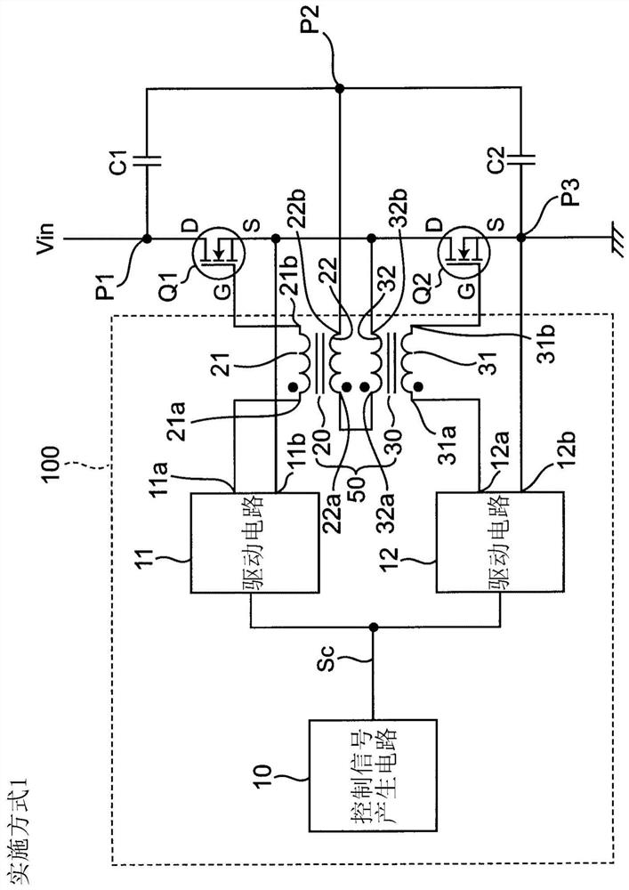
[0040] figure 1 It is a circuit diagram showing a configuration example of the switching circuit 100 and its peripheral circuits in the first embodiment. exist figure 1 Among them, the switching circuit 100 includes a control signal generating circuit 10 , a pair of driving circuits 11 and 12 , and a pair of transformers 20 and 30 . Here, a pair of transformers 20, 30 constitutes a voltage balance circuit 50 for obtaining a voltage balance of the semiconductor device Q1 when a switching control signal is applied to each gate (control terminal) of the pair of semiconductor devices Q1, Q2. , The voltage balance of the voltage (output voltage) between the drain (first element terminal) and source (second element terminal) of Q2.

[0041] exist figure 1 Among them, the semiconductor devices Q1 and Q2 are, for example, N-channel MOS field effect transistors, and are connected in series with each other. That is, the input voltage Vin is applied to the drain of the semiconductor ...

Embodiment approach 2

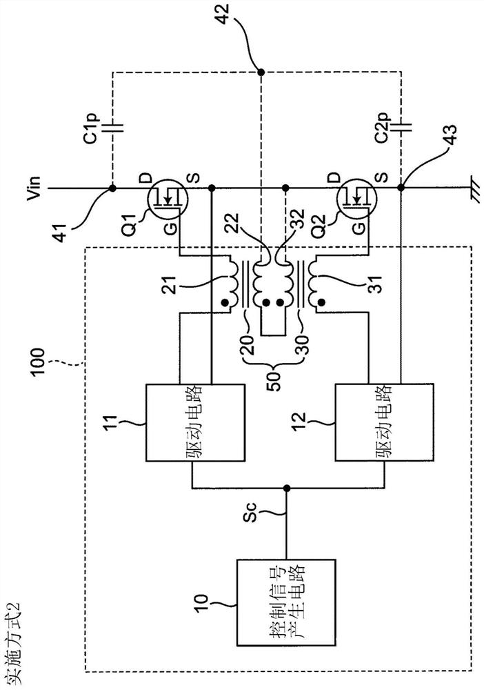
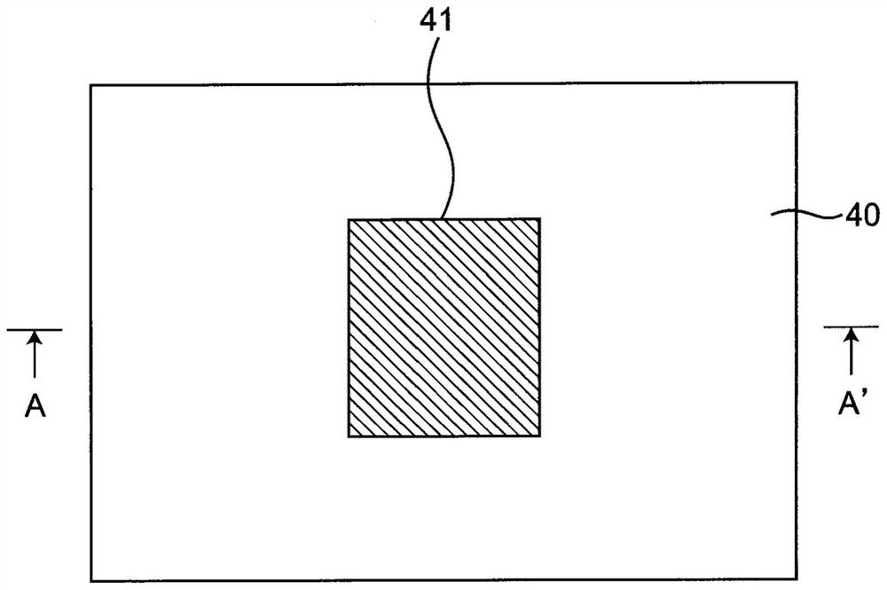
[0048] figure 2 It is a circuit diagram showing a configuration example of the switching circuit 100 and its peripheral circuits according to the second embodiment. also, Figure 3A yes figure 2 A top view of the electrode 41 portion, Figure 3B its about Figure 3A A longitudinal sectional view of line A-A'. figure 2 The peripheral circuit of the switching circuit 100 with figure 1 Compared with the peripheral circuit of the present invention, it is characterized in that the capacitors C1 and C2 are replaced by the parasitic capacitors C1p and C2p, respectively.

[0049] Specifically, as Figure 3A and Figure 3B As shown, the parasitic capacitance C1p is parasiticly formed between a pair of electrodes 41, 42 sandwiching the dielectric substrate 40 on which the semiconductor devices Q1, Q2 are mounted and the electrodes are opposed to each other, and the parasitic capacitance C2p Similar to the parasitic capacitance C1p, it is parasiticly formed between a pair of e...

Embodiment approach 3

[0054] Figure 5 It is a circuit diagram showing a configuration example of a power conversion device according to Embodiment 3. Figure 5 The power conversion device is used with figure 1 The switching circuit 100 of the voltage balancing circuit 50 is an asynchronous rectification type boost chopper circuit.

[0055] exist Figure 5 In the above, the input voltage Vin from the DC voltage source 1 is applied to the series circuit of the semiconductor devices Q1, Q2 via the reactor Lr. The drain of the semiconductor device Q1 is connected to the smoothing electrolytic capacitor Cb and the load resistor 2 via the rectifier diode D1.

[0056] In the power conversion device configured as above, the input voltage Vin can be boosted by asynchronous rectification and output to the load resistor 2 . In addition, the operation and effect of the voltage balance circuit 50 are the same as those of the first and second embodiments.


PUM


Abstract

A voltage balancing circuit including first and second semiconductor devices connected in series with each other, includes a first transformer having a primary winding and a secondary winding, a second transformer having a primary winding and a secondary winding, and a pair of capacitors connected in series with each other and connected between output terminals of the plurality of semiconductor devices. A first control signal is applied to the control terminal of the first semiconductor device via the primary winding of the first transformer, a second control signal is applied to the control terminal of the second semiconductor device via the primary winding of the second transformer, and one ends of the secondary windings are connected to each other.

Description

technical field [0001] The present invention relates to, for example, a voltage balancing circuit for a plurality of semiconductor devices connected in series, and a switching circuit and a power conversion device using the voltage balancing circuit. Background technique [0002] For example, by connecting a plurality of semiconductor devices as switching elements in series, using them as a single element, and synchronously turning on and off the switches, a switch with high withstand voltage characteristics can be realized with a low withstand voltage device circuit. Here, since a semiconductor device with a low breakdown voltage is significantly cheaper than a semiconductor device with a high breakdown voltage, and its on-resistance is also small, it is possible to achieve low cost and high operating efficiency. However, due to variations in the electrical characteristics of semiconductor devices, the voltage balance may be disrupted and the voltage design standards may b...

Claims


Application Information

Patent Timeline
Patent Type & Authority Applications(China)
IPC IPC(8): H02M1/00H02M1/08
CPCH02M1/088H02M3/155H02M7/5387H03K17/102H02M7/537
Inventor 野坂纪元冈田亘陈晨石井隆章
Owner ORMON CORP
Why Eureka
Try Eureka