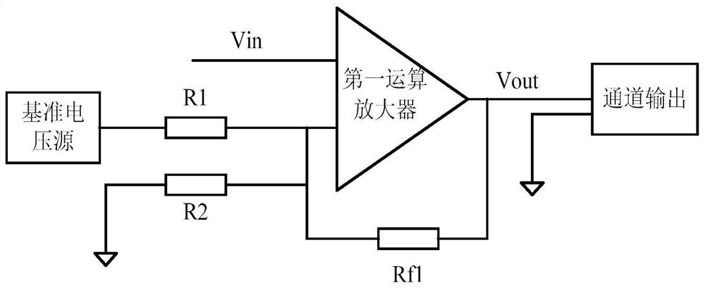
Configurable voltage output device and method based on discrete semiconductors and controller
A voltage output and semiconductor technology, applied in the field of configurable voltage output devices, can solve problems such as single output range, inconvenient improvement, and inability to meet terminal instrument control, and achieve low cost and easy improvement effects
- Summary
- Abstract
- Description
- Claims
- Application Information
AI Technical Summary
Problems solved by technology
Method used
Image
Examples
Embodiment 1
[0041] figure 1 It is a schematic structural diagram of a configurable voltage output device based on discrete semiconductors in Embodiment 1 of the present application, such as figure 1 As shown, the device includes: a PWM signal generation module 1, a voltage configuration module 2, a frequency selection module 3, and an operation module 4;
[0042] The PWM signal generation module 1 is connected with the voltage configuration module 2 for generating a PWM signal and outputting it to the voltage configuration module 2; the frequency and duty cycle of the PWM signal are determined based on the accuracy and range of the required output voltage;
[0043] The voltage configuration module 2 is connected with the frequency selection module 3 for receiving the PWM signal, obtains the first pulse signal by changing the duty cycle of the PWM signal, and outputs the first pulse signal to the frequency selection module 3; wherein, the duty cycle is based on The output voltage range of...
Embodiment 2
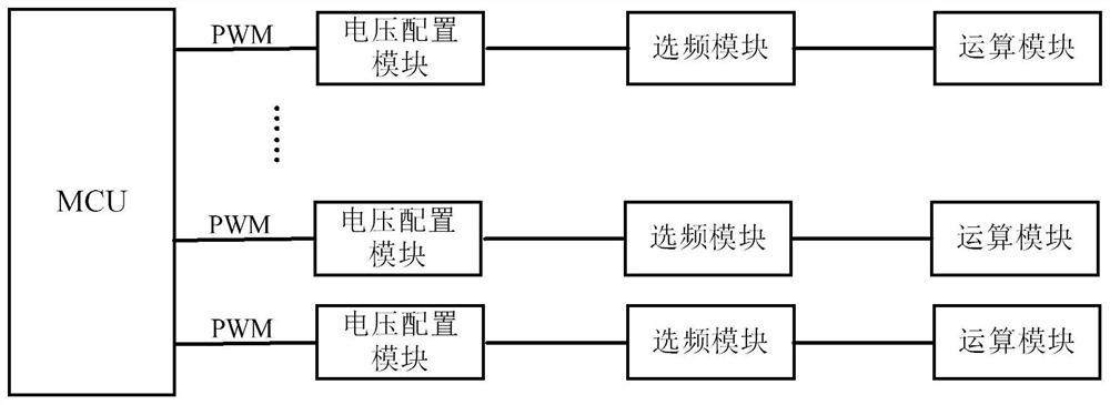
[0058] image 3 It is a schematic structural diagram of a multi-channel discrete semiconductor-based configurable voltage output device provided in Embodiment 2 of the present application, as shown in image 3 As shown, the present application provides a multi-channel discrete semiconductor-based configurable voltage output device through Embodiment 2. Since a single type of voltage output type cannot meet multi-industry applications, this embodiment adopts a voltage output device for different terminal control requirements. The configuration module adjusts the output voltage range. Among them, the control signal of the channel voltage is controlled by the PWM signal, and the duty ratio of the PWM signal is adjusted through the voltage configuration module, so as to realize the control of the controlled terminal with multiple voltage ranges. Specifically, the MCU uses the 32-bit microcontroller SC32F19128LM1G produced by Silan Microelectronics, which can output voltages rangi...
Embodiment 3
[0061] This embodiment provides a configurable voltage output device based on discrete semiconductors with line impedance compensation. The following will combine Figure 4 The line impedance compensation involved in this embodiment will be described in detail.
[0062] Figure 4 It is a schematic diagram of the circuit structure of the circuit impedance compensation for the voltage output device provided in the third embodiment of the present application; Figure 4 As shown, this part is composed of a differential proportional operation circuit, a pull-up circuit, and a voltage follower circuit. The differential proportional operation circuit is composed of the second operational amplifier, the third resistor R3, the fourth resistor R4, the fifth resistor R5, and the second feedback resistor Rf2, the input terminal u1 and the input terminal u2 are connected to the line impedance compensation terminal, and the third resistor R3 Both ends are respectively connected to the in...
PUM
 Abstract
Description
Claims
Application Information


