Array substrate, driving chip and display device

A technology for array substrates and display areas, applied to static indicators, instruments, etc., can solve problems such as horizontal and vertical stripes, uneven brightness and darkness, and lower reliability of display devices

Pending Publication Date: 2021-04-16
XIAMEN TIANMA MICRO ELECTRONICS
View PDF0 Cites 2 Cited by
  • Summary
  • Abstract
  • Description
  • Claims
  • Application Information

AI Technical Summary

Problems solved by technology

When the resistance difference between different lead wires is large, the probability of poor display of the display device will increase, which will easily cause di

Method used


Image

  • Array substrate, driving chip and display device
  • Array substrate, driving chip and display device
  • Array substrate, driving chip and display device

Examples


Embodiment Construction

[0026] The present invention will be further described in detail below in conjunction with the accompanying drawings and embodiments. It should be understood that the specific embodiments described herein are only used to explain the present invention, but not to limit the present invention. In addition, it should be noted that, for the convenience of description, the drawings only show some but not all structures related to the present invention.

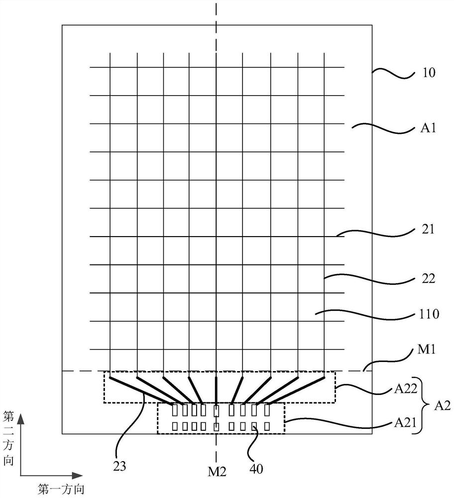
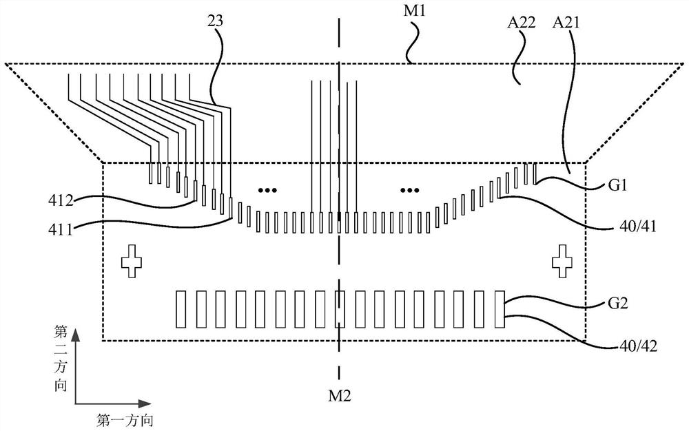
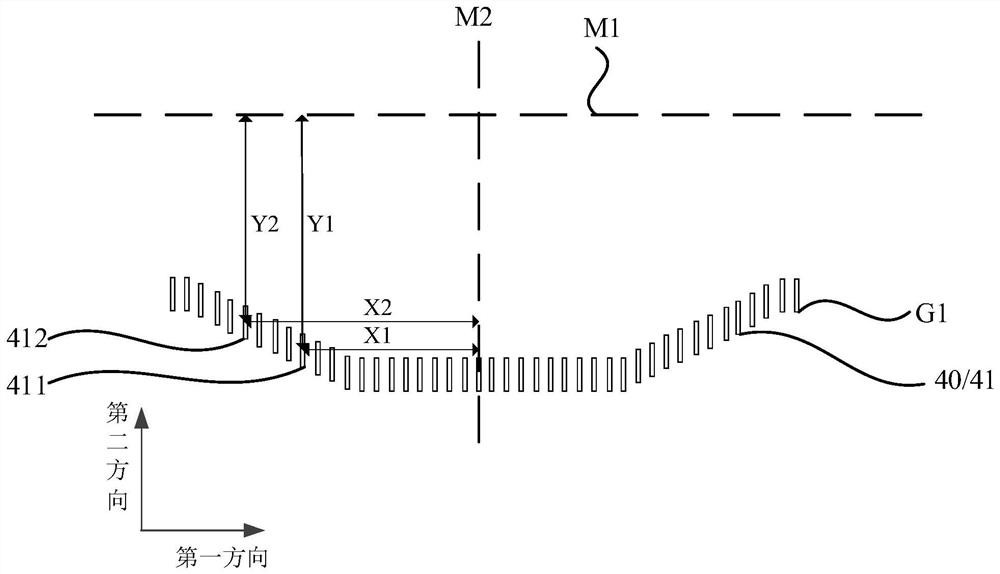
[0027] figure 1 A schematic top-view structure diagram of an array substrate provided by an embodiment of the present invention, figure 2 for figure 1 The schematic top-view structure of the stepped area of ​​the array substrate shown in , image 3 for figure 2 The schematic top view structure of the output pad group in the step area shown in , refer to Figure 1-Figure 3 , the array substrate includes a display area A1 and a step area A2, and a boundary line M1 is formed at the adjoining position of the display area A1 and...


PUM


Abstract

The invention provides an array substrate, a driving chip and a display device, the array substrate comprises a display area and a step area, a boundary line is formed at the adjacent position of the display area and the step area, and the step area comprises a binding area; a plurality of pads, wherein the plurality of gaskets comprise at least one output gasket group, and the output gasket group comprises a plurality of output gaskets; the plurality of output gaskets comprise a first gasket and a second gasket, the first gasket and the second gasket are located in the same output gasket group, the vertical distance between the first gasket and the central axis is smaller than the vertical distance between the second gasket and the central axis, and the vertical distance between the first gasket and the boundary line is larger than the vertical distance between the second gasket and the boundary line; the central axis passes through the center of the boundary line, and the first direction intersects with the central axis. According to the embodiment of the invention, the length of the data connecting line connected with the first gasket is close to the length of the data connecting line connected with the second gasket as much as possible, so that the length difference between the data connecting lines is reduced, and the display quality is improved.

Description

technical field [0001] The present invention relates to the field of display technology, and in particular, to an array substrate, a driving chip and a display device. Background technique [0002] In a current common display device, leads need to be arranged in the peripheral circuit area on the array substrate to connect the display area and the integrated circuit. For example, a plurality of lead wires are required to connect the signal lines of the display area to the display driver chip. [0003] In the existing array substrate, the leads are all arranged with the same material, thickness and line width, and it can be known from the resistance law that the resistance of each lead is proportional to its length. For multiple leads connected to the same chip, since the size of the chip is usually smaller than the size of the display area, it is difficult to ensure that the lengths of all leads are the same when arranging the leads, which is usually the same as that of the ...

Claims


Application Information

Patent Timeline
IPC IPC(8): G09G3/20
Inventor 纪文套庄知龙黄建才
Owner XIAMEN TIANMA MICRO ELECTRONICS
Why Eureka
Try Eureka