
A method for collimating solid-state light emitting chip or chip array light source

A solid-state light emitting and chip array technology, applied in the field of projection display, can solve the problems of increasing the difficulty of coating, unfavorable miniaturization, loss of light energy, etc., and achieve the effect of achieving collimation effect, increasing the scope of application, and improving the transmittance

Active Publication Date: 2022-02-01
SICHUAN CHANGHONG ELECTRIC CO LTD
View PDF10 Cites 0 Cited by
  • Summary
  • Abstract
  • Description
  • Claims
  • Application Information

AI Technical Summary

Problems solved by technology

The surface type of the traditional collimating lens group is generally a convex lens or even an aspheric surface. The collimation is achieved by adjusting the curvature, thickness, and spacing. To improve the utilization rate of light energy, it is necessary to manufacture a high-precision lens group, which will increase the aperture. Improving the processing technology is not conducive to miniaturization, and if you want to reduce the volume, you will inevitably lose light energy. You cannot have both, and you must make a trade-off
And convex lens or aspheric surface will also increase the difficulty of coating
In addition, it is difficult to integrate collimating lens group components with solid-state light-emitting chips or chip-array light sources

Method used


Image

  • A method for collimating solid-state light emitting chip or chip array light source
  • A method for collimating solid-state light emitting chip or chip array light source
  • A method for collimating solid-state light emitting chip or chip array light source

Examples


Embodiment 1

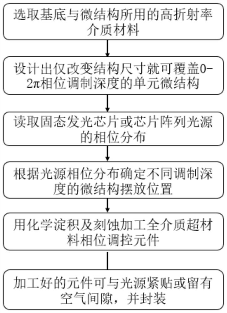
[0034] A method for collimating a solid-state light-emitting chip or a chip-array light source, by using an all-dielectric metamaterial phase control element to realize the collimation effect on a solid-state light-emitting chip or a chip-array light source, can eliminate the use of traditional lens components. Such as figure 1 As shown, it specifically includes the following steps:

[0035] Step 1. Select a dielectric material for making a substrate and a microstructure, and the substrate is used to support the microstructure.

[0036] Both the substrate and the microstructure of this solution use high-transmittance dielectric materials, so there is no need to coat them like lens groups to improve the light source transmittance.

[0037] Step 2. Design the microstructure.

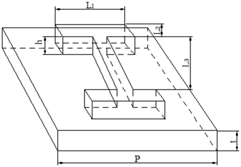
[0038] The microstructure can cover 0-2π phase modulation depth only by changing the structure size, and the microstructure can be designed for broadband phase modulation; then it can be applied to colli...

Embodiment 2

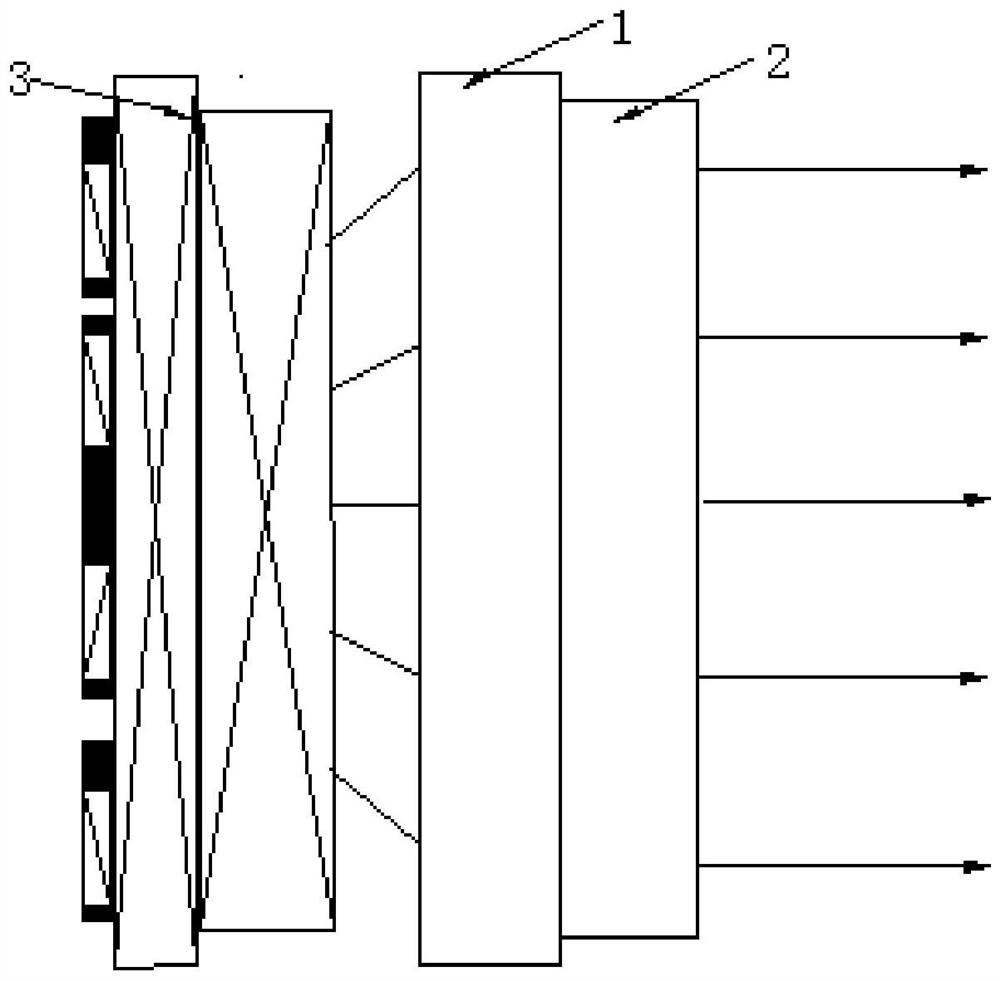
[0053] The difference between this embodiment and Embodiment 1 is that in this embodiment, if Figure 7 to Figure 8 As shown, the microstructure arrays are arranged on both sides of the substrate according to the position of a specific phase modulation depth, and the positions of the microstructure arrays on both sides are staggered.


PUM


Abstract

The invention discloses a method for collimating a solid-state light-emitting chip or a chip array light source, which includes the following steps: selecting a dielectric material for making a substrate and a microstructure; designing a microstructure, and the microstructure can cover 0‑ 2π phase modulation depth; read the phase distribution of solid-state light-emitting chips or chip array light sources; determine the placement position of microstructures with different modulation depths according to the phase distribution of light sources; process all-dielectric metamaterial phase control elements, and the phase control components include substrates and microstructure; package the processed phase control element and light source. The method of the invention can improve the light collection efficiency, reduce the element size, and can integrate the phase control element and the light source together.

Description

technical field [0001] The invention relates to the technical field of projection display, in particular to a method for collimating a solid-state light emitting chip or a chip array light source. Background technique [0002] Existing projection systems generally use lens assemblies to collimate solid-state light emitting chips or chip array light sources. The surface type of the traditional collimating lens group is generally a convex lens or even an aspheric surface. The collimation is achieved by adjusting the curvature, thickness, and spacing. To improve the utilization rate of light energy, it is necessary to manufacture a high-precision lens group, which will increase the aperture. Improving the processing technology is not conducive to miniaturization, and if you want to reduce the volume, you will inevitably lose light energy. You cannot have both, and you must make a trade-off. And the convex lens or aspheric surface will also increase the difficulty of coating. ...

Claims


Application Information

Patent Timeline
Patent Type & Authority Patents(China)
IPC IPC(8): G03B21/20
Inventor 张源杨雄康健
Owner SICHUAN CHANGHONG ELECTRIC CO LTD
Learn More