Three-dimensional and flash memory and manufacturing method thereof

A manufacturing method and memory technology, applied in semiconductor/solid-state device manufacturing, electric solid-state devices, semiconductor devices, etc., can solve the problem of less use of AND flash memory

Pending Publication Date: 2021-04-20
MACRONIX INT CO LTD
View PDF0 Cites 0 Cited by
  • Summary
  • Abstract
  • Description
  • Claims
  • Application Information

AI Technical Summary

Problems solved by technology

[0003] At present, the flash memory commonly used in the industry includes NOR flash memory and NAND flash memory, but the use of AND flash memory is less

Method used


Image

  • Three-dimensional and flash memory and manufacturing method thereof
  • Three-dimensional and flash memory and manufacturing method thereof
  • Three-dimensional and flash memory and manufacturing method thereof

Examples


Embodiment Construction

[0043] In order to make the object, technical solution and advantages of the present invention clearer, the present invention will be described in further detail below in conjunction with specific embodiments and with reference to the accompanying drawings.

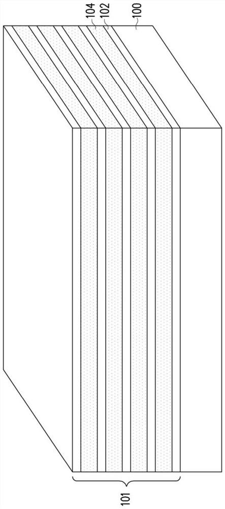
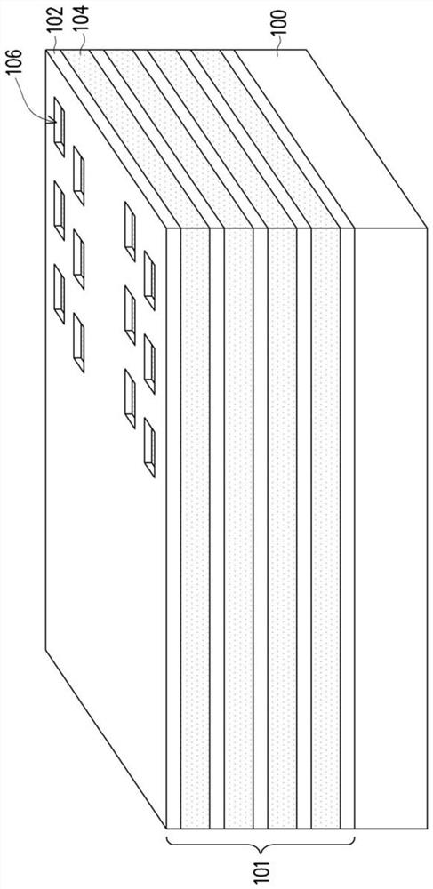
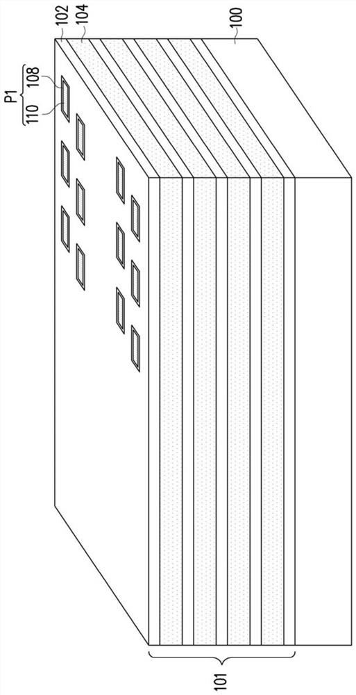
[0044] Figure 1A to Figure 1L It is a schematic diagram of a manufacturing method of a three-dimensional flash memory according to an embodiment of the present invention. figure 2 yes Figure 1I side view diagram.

[0045] Please refer to Figure 1A , forming a stacked structure 101 on the substrate 100 . The substrate 100 may be, for example, a semiconductor substrate, for example, the substrate 100 may be a silicon substrate. In some embodiments, a doped region (for example, an N+ doped region or an N-type well region) can be formed in the substrate 100 according to design requirements. In other embodiments, a buried oxide layer (not shown) may be further formed on the substrate 100 . In this embodiment, the subs...


PUM


Abstract

The invention discloses a three-dimensional and flash memory and a manufacturing method thereof. The manufacturing method comprises the following steps of forming a stacked structure including alternately stacked first insulating layers and first sacrificial layers; forming a first pillar structure penetrating through the stack structure and including a second insulating layer and a second sacrificial layer surrounding the second insulating layer; forming a second column structure which penetrates through the laminated structure and comprises a channel layer and an insulating column surrounding the channel layer, wherein the second sacrificial layers are located at the two sides of the channel layer; removing the first sacrificial layer to form a lateral opening exposing a portion of the second insulating layer and the channel layer; and forming a gate dielectric layer surrounding the exposed second insulating layer and the channel layer in the lateral opening; filling a gate layer in the lateral opening; and replacing the second sacrificial layer with a conductor layer.

Description

technical field [0001] The present invention relates to a three-dimensional flash memory and its manufacturing method, and in particular to a three-dimensional flash memory and its manufacturing method. Background technique [0002] Non-volatile memory (such as flash memory) has the advantage that the stored data will not disappear even after power off, so it has become a kind of memory widely used in personal computers and other electronic devices. [0003] At present, the flash memory commonly used in the industry includes a negative-or (NOR) flash memory and a negative-and-type (NAND) flash memory, but the use of and-type (AND) flash memory is seldom. Since the AND flash memory can also be applied in a multi-dimensional flash memory cell array, it has the same degree of integration and area utilization as the NAND flash memory. Therefore, the development of flash memory has become the current trend. Contents of the invention [0004] The invention provides a method fo...

Claims


Application Information

Patent Timeline
Patent Type & Authority Applications(China)
IPC IPC(8): H01L27/11551H01L27/11578
CPCH01L29/40117H01L21/31144H10B43/40H10B43/50H10B43/20H01L21/02164H01L21/02636H01L21/0217H01L21/31111H01L29/513H01L29/518H10B43/27H10B43/10
Inventor 胡志玮叶腾豪江昱维
Owner MACRONIX INT CO LTD
Why Eureka
Try Eureka