Antenna packaging structure and packaging method

An encapsulation method and encapsulation structure technology, which are applied in the directions of antenna support/installation device, antenna grounding switch structure connection, antenna, etc., can solve the problems of difficult to effectively protect the chip and large size of the antenna package.

Pending Publication Date: 2021-04-27
SJ SEMICON JIANGYIN CORP
View PDF0 Cites 2 Cited by
  • Summary
  • Abstract
  • Description
  • Claims
  • Application Information

AI Technical Summary

Problems solved by technology

[0006] In view of the above-mentioned shortcomings of the prior art, the object of the present invention is to provide an antenna packaging structure and packaging method, which are used to solve the problems in the prior art that the antenna packaging volume is large, the chip is difficult to be effectively protected, and the package is simple and stable.

Method used


Image

  • Antenna packaging structure and packaging method
  • Antenna packaging structure and packaging method
  • Antenna packaging structure and packaging method

Examples


Embodiment 1

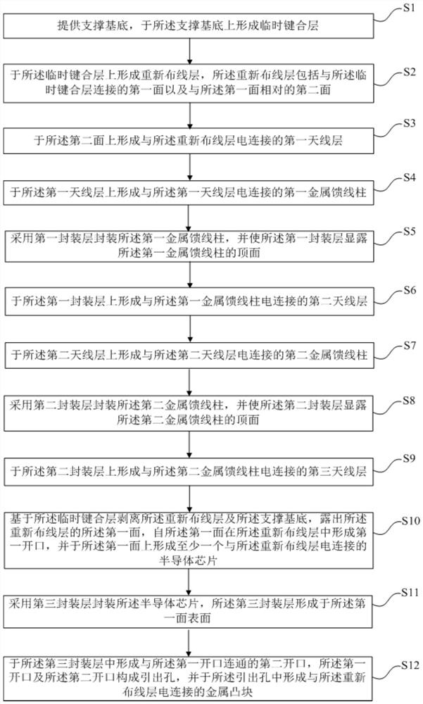
[0107] Such asfigure 1 As shown, the present invention provides a kind of antenna packaging method, and described packaging method comprises steps:

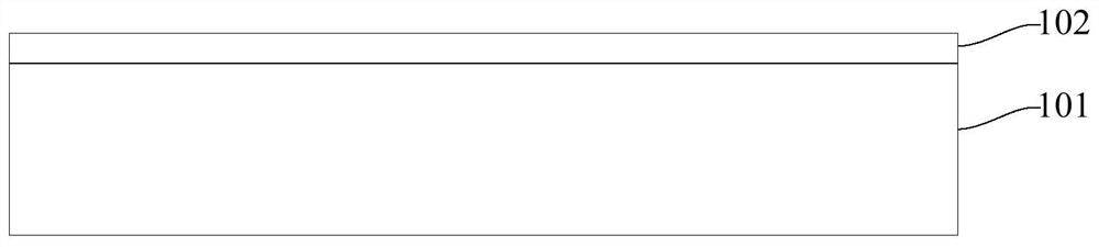
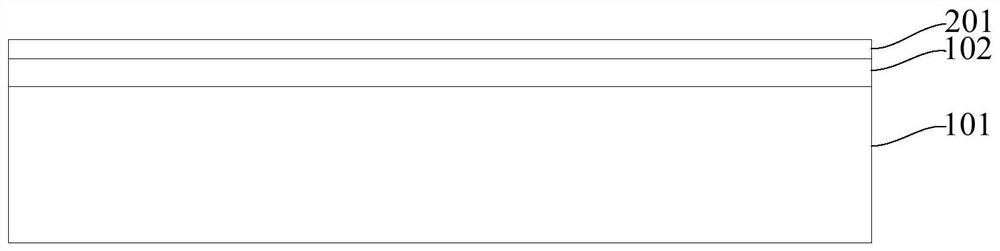
[0108] providing a support base on which a temporary bonding layer is formed;

[0109] forming a rewiring layer on the temporary bonding layer, the rewiring layer including a first surface connected to the temporary bonding layer and a second surface opposite to the first surface;

[0110] forming a first antenna layer electrically connected to the redistribution layer on the second surface;

[0111] forming a first metal feeder post electrically connected to the first antenna layer on the first antenna layer;

[0112] encapsulating the first metal feeder column with a first encapsulation layer, and exposing the top surface of the first metal feeder column by the first encapsulation layer;

[0113] forming a second antenna layer electrically connected to the first metal feeder post on the first packaging layer;

[0114] formin...

Embodiment 2

[0165] Such as Figure 23 shown, and see Figures 1 to 22 , the present invention also provides an antenna packaging structure, wherein the antenna packaging structure is preferably packaged by the antenna packaging method of the present invention, of course, the antenna packaging structure can also be packaged by other packaging methods, the antenna package Structures include:

[0166] a rewiring layer, the rewiring layer includes a first surface and a second surface opposite to the first surface, and a first opening 501 opened from the first surface is formed in the rewiring layer;

[0167] a first metal feeder post 303, formed on the first antenna layer 301 and electrically connected to the first antenna layer 301;

[0168] The first encapsulation layer 305 covers the first metal feeder post 303 , and the first encapsulation layer 305 exposes the top surface of the first metal feeder post 303 ;

[0169] The second antenna layer 307 is formed on the first encapsulation la...


PUM


Abstract

The invention provides an antenna packaging structure and a packaging method. The packaging method comprises the steps of providing a supporting substrate, and forming a rewiring layer, a first antenna layer, a first metal feeder column, a first packaging layer, a second antenna layer, a second metal feeder column, a second packaging layer, a third antenna layer, a semiconductor chip, a metal bump and a third packaging layer. The semiconductor chip is protected based on the third packaging layer, the chip and the metal bump are packaged at the same time, the stability of the packaging structure can be effectively improved, the holes are formed in the packaging layer firstly, then the metal bump is formed, the process is simplified, preparation of the metal bump is facilitated, and the multilayer antenna structure is formed through the multiple metal feeder columns and the multiple packaging layers. The packaging size is reduced, the signal receiving capability is enhanced, the signal receiving bandwidth is expanded, the bottom filling layer is formed, the packaging stability is improved, the box dam dispensing process is added, the stability of the chip is improved, dual protection is carried out on the chip, the packaging process flow can be effectively reduced, and the process period is prolonged.

Description

technical field [0001] The invention belongs to the field of packaging and the field of communication equipment, and in particular relates to an antenna packaging structure and a packaging method. Background technique [0002] Due to the progress of science and technology, various high-tech electronic products have been developed to facilitate people's life, including various electronic devices, such as notebook computers, mobile phones, tablet computers (PADs), and the like. [0003] With the popularization of these high-tech electronic products and the increase of people's demand, in addition to the substantial increase of various functions and applications configured in these high-tech products, especially in order to meet people's mobile needs, the function of wireless communication has been added. Therefore, people can use these high-tech electronic products at any place or at any time through these high-tech electronic devices with wireless communication functions. Th...

Claims


Application Information

Patent Timeline
Patent Type & Authority Applications(China)
IPC IPC(8): H01L21/56H01L21/60H01L23/485H01L23/31H01L25/18H01Q1/22H01Q1/38H01Q1/50
CPCH01L21/56H01L23/3107H01L24/02H01L24/03H01L25/18H01L2224/0231H01L2224/02331H01L2224/02379H01L2224/02381H01L2224/031H01Q1/2283H01Q1/38H01Q1/50
Inventor 吴政达陈彦亨林正忠薛亚媛徐罕
Owner SJ SEMICON JIANGYIN CORP
Why Eureka
Try Eureka