Printed circuit board, display module and LED display screen

A technology of LED display screen and printed circuit board, which is applied in the direction of printed circuit, printed circuit parts, printed circuit connected with non-printed electrical components, etc. PCB pad position offset and other issues

Active Publication Date: 2021-04-30
SHENZHEN ABSEN OPTOELECTRONIC CO LTD
View PDF5 Cites 1 Cited by
  • Summary
  • Abstract
  • Description
  • Claims
  • Application Information

AI Technical Summary

Problems solved by technology

During the current placement process, the following abnormal situations will occur: During the solder paste printing process, the position of the solder paste and the solder pad on the PCB is offset due to insufficient printing accuracy of the solder paste.
The above situation will lead to yin-yang screen, and as the pixel pitch becomes smaller and smaller, the position accuracy requirements between the PCB pad and solder paste are getting higher and higher, and the resulting yin-yang screen problem is becoming more and more serious

Method used


Image

  • Printed circuit board, display module and LED display screen
  • Printed circuit board, display module and LED display screen
  • Printed circuit board, display module and LED display screen

Examples


specific Embodiment approach

[0067] The first implementation mode:

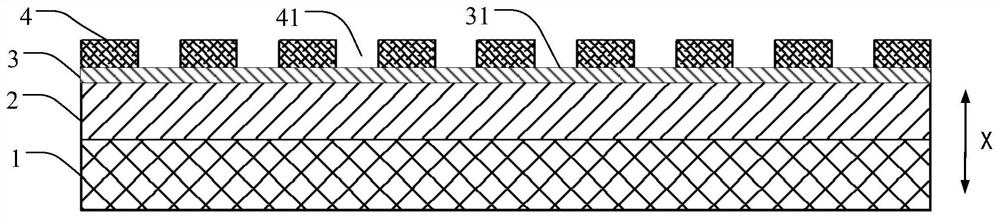
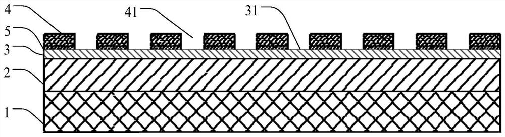
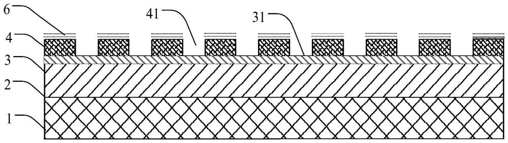
[0068] see Figure 4 ,and Figure 4 The direction in is for reference. It can be seen that the printed circuit board includes the fourth prepreg layer, the first copper foil layer 3, the first prepreg layer 2, the copper clad laminate layer 1, the second prepreg layer 7, and the second copper foil layer stacked in sequence from top to bottom. Foil layer 8 and fifth prepreg layer. That is, in this embodiment, the first insulating layer 4 is the fourth prepreg layer, and the second insulating layer 9 is the fifth prepreg layer.

[0069]The first copper foil layer 3 has a first pad 31 , and the fourth prepreg layer is provided with a first through hole 41 penetrating through the thickness direction; the first pad 31 is located in the first through hole 41 . The second copper foil layer 8 has a second pad 81 , and the fifth prepreg layer is provided with a fourth through hole 91 penetrating through the thickness direction; the second pad ...


PUM


Abstract

The invention discloses a printed circuit board, a display module and an LED display screen. The display module comprises the printed circuit board, and the printed circuit board comprises a copper-clad plate layer, a first prepreg layer, a first copper foil layer and a first insulating layer which are stacked in sequence from bottom to top; the first copper foil layer is provided with a first bonding pad, and the first insulating layer is provided with a first through hole penetrating in the thickness direction; and the first bonding pad is located in the first through hole. When the display module is manufactured, soldering paste can be arranged in the first through hole, the positions of the first bonding pad and the soldering paste are relatively fixed under the limiting effect of the inner side wall of the first through hole, and the situation that the positions of the soldering paste and the first bonding pad deviate is avoided. Therefore, when the soldering paste is arranged, the inner side wall of the first through hole plays a role in limiting, the printing precision of the soldering paste is improved, and the problems of yin and yang screens of the display screen caused by position deviation of the bonding pad and the soldering paste are solved.

Description

technical field [0001] The present application relates to the field of display technology, in particular to a printed circuit board, a display module and an LED display. Background technique [0002] LED (light emitting diode, light-emitting diode) display screens have the advantages of wide color gamut, high brightness, large viewing angle, low power consumption, and long service life. Therefore, in the display field, LED display screens are widely used. [0003] With the development of LED display screens, the improvement of its pixel pitch and optical performance has always been the focus of attention in the industry. Among them, the pixel pitch is getting smaller and smaller is a major development trend. However, as the pixel pitch shrinks, the process difficulty of the LED display screen increases, and the optical performance of the LED display screen cannot be guaranteed. Among them, the most common problem is the occurrence of yin-yang screens; for example, for a dis...

Claims


Application Information

Patent Timeline
Patent Type & Authority Applications(China)
IPC IPC(8): H05K1/11H05K1/18G09F9/33
CPCH05K1/111H05K1/181G09F9/33
Inventor 徐梦梦
Owner SHENZHEN ABSEN OPTOELECTRONIC CO LTD
Why Eureka
Try Eureka