
Phase shifter plate welding debugging method with PIM requirement

A debugging method and a technology of a phase shifter, which are applied in connection, line/collector components, metallurgical combination, etc., can solve problems such as poor welding debugging accuracy, unreasonable welding debugging methods, and inconsistent welding debugging methods, and achieve improved The effect of precision

Pending Publication Date: 2021-04-30
SHENZHEN SUN & LYNN CIRCUITS
View PDF4 Cites 0 Cited by
  • Summary
  • Abstract
  • Description
  • Claims
  • Application Information

AI Technical Summary

Problems solved by technology

[0008] (1) In terms of welding debugging, the existing welding debugging methods in the industry are not uniform, and there is no relevant high-reliability method to refer to
[0009] (2) The existing welding debugging method is unreasonable, it is easy to produce stress residue, the value fluctuates greatly during the PIM test, and the accuracy of welding debugging is poor
[0010] The difficulty of solving the above problems and defects is: unreasonable welding debugging method can easily produce stress residue, and there are many sources of stress during welding, such as the terminal is not stable during welding, the wire and terminal have a certain angle after welding, and the soldering tin surface is uneven etc., but the welding stress mainly comes from the pulling of the wire to the welding terminal, especially the release of the internal stress accumulated in the wire itself, and the internal stress of the wire itself mainly comes from the winding and folding of the wire itself, which is uncertain, so the solution to welding The most important thing about stress residue is to avoid the pulling of the solder terminal by the stress release of the wire itself

Method used


Image

  • Phase shifter plate welding debugging method with PIM requirement
  • Phase shifter plate welding debugging method with PIM requirement
  • Phase shifter plate welding debugging method with PIM requirement

Examples


Embodiment Construction

[0042] In order to make the object, technical solution and advantages of the present invention more clear, the present invention will be further described in detail below in conjunction with the examples. It should be understood that the specific embodiments described here are only used to explain the present invention, not to limit the present invention.

[0043] Aiming at the problems existing in the prior art, the present invention provides a welding debugging method for a phase shifter board requiring PIM. The present invention will be described in detail below in conjunction with the accompanying drawings.

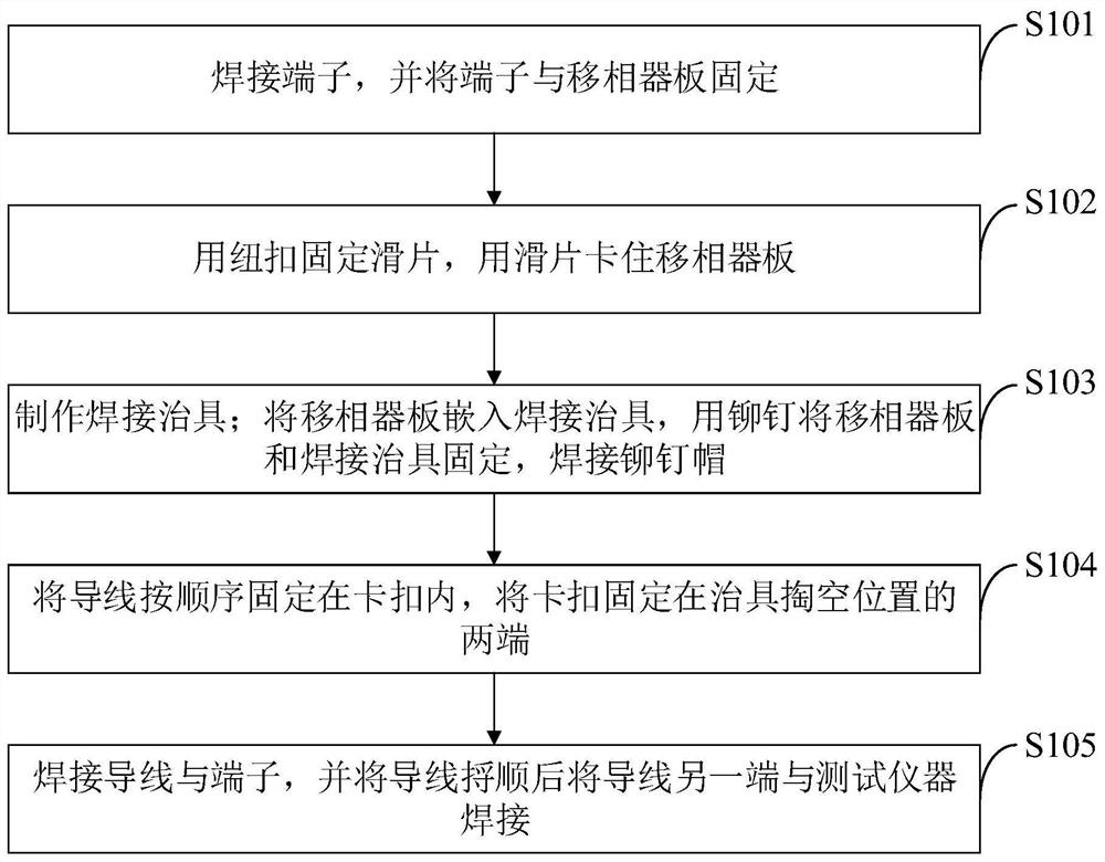
[0044] Such as figure 1 As shown, the PIM-required phase shifter board welding debugging method provided by the embodiment of the present invention includes the following steps:

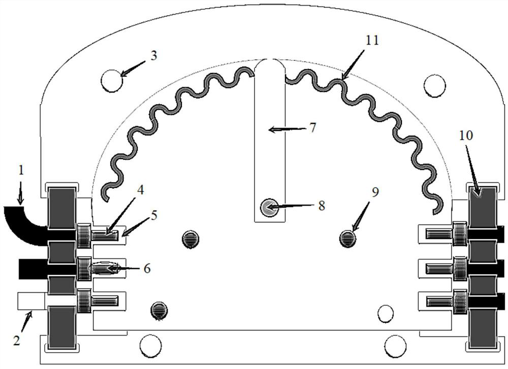
[0045] S101, solder terminal 4, and fix terminal 4 with the phase shifter board;

[0046] S102, fix the slider 7 with the button 8, and clamp the phase shifter board with the slider 7;

...


PUM


Abstract

The invention belongs to the technical field of 4G / 5G radio frequency antenna circuit boards, and discloses a phase shifter board welding debugging method with PIM requirements, which comprises the following steps: welding a terminal, and fixing the terminal with a phase shifter board; fixing the slip sheet by using a button, and clamping the phase shifter plate by using the slip sheet; manufacturing a welding jig; embedding the phase shifter plate into the welding jig, fixing the phase shifter plate and the welding jig by using rivets, and welding the rivet caps; successively fixing the wires in the buckles, and fastening the buckles to the two ends of the hollowed-out position of the jig; and welding the wire and the terminal, smoothing the wire, and then welding the other end of the wire with a test instrument. By carding the welding sequence and designing welding auxiliary accessories, stress residues generated when the phase shifter circuit board with the PIM requirement is welded and debugged can be effectively controlled, the welding and debugging precision of the phase shifter circuit board with the PIM requirement is much higher than that of an existing process, the influence of the welding stress residues on PIM testing is greatly reduced, and thereby the precision of the PIM testing is improved.

Description

technical field [0001] The invention belongs to the technical field of 4G / 5G radio frequency antenna circuit boards, and in particular relates to a welding debugging method for a phase shifter board required by PIM. Background technique [0002] At present, as the frequency and rate of signal transmission increase, a circuit board with PIM (passive intermodulation) requirements appears in the industry. Passive intermodulation PIM is caused by the nonlinear characteristics of various passive components in the antenna transmission system. In high-power, multi-channel systems, due to their high-power characteristics, traditional passive linear devices have strong nonlinear effects. The nonlinearity of these passive devices will generate higher harmonics relative to the operating frequency. These harmonics mix with the operating frequency to create a new set of frequencies, with the end result being an unwanted spectrum. [0003] In order to ensure that high-frequency and high...

Claims


Application Information

Patent Timeline
IPC IPC(8): H05K3/34H01R43/02
CPCH05K3/3405H01R43/0256H01R43/0263H05K2203/04
Inventor 李旋吴传亮常玉兵王运玖周建军
Owner SHENZHEN SUN & LYNN CIRCUITS
Learn More