Micro light-emitting element array substrate, and preparation method and transfer method thereof

An array substrate and micro-light emitting technology, which is applied in the fields of electrical components, semiconductor/solid-state device manufacturing, and electric solid-state devices, etc., can solve the problems of small distance between micro-LEDs, small size of micro-LEDs, and difficult substrate peeling process, etc. The effect of preventing incomplete peeling and facilitating peeling

Active Publication Date: 2021-05-04
CHENGDU VISTAR OPTEOLECTRONICS CO LTD
View PDF10 Cites 3 Cited by
  • Summary
  • Abstract
  • Description
  • Claims
  • Application Information

AI Technical Summary

Problems solved by technology

However, due to the small size of micro-light emitting diodes and the small distance between adjacent micro-light-emitting diodes, there are many difficulties in the manufacture of micro-light-emitting diodes, such as the peeling process of the substrate.

Method used


Image

  • Micro light-emitting element array substrate, and preparation method and transfer method thereof
  • Micro light-emitting element array substrate, and preparation method and transfer method thereof
  • Micro light-emitting element array substrate, and preparation method and transfer method thereof

Examples


preparation example Construction

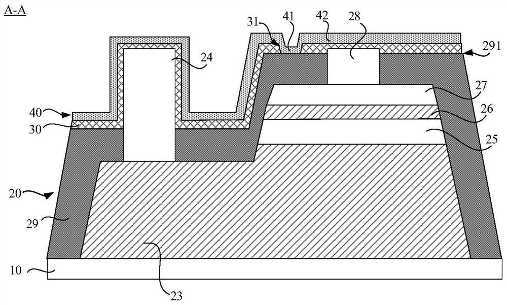
[0072] An embodiment of the present invention provides a method for preparing a micro-LED array substrate, comprising the following steps:

[0073] S110, providing a substrate;

[0074] S120, forming a micro light emitting diode chip on the substrate, the surface of the micro light emitting diode chip facing away from the substrate is a connection surface;

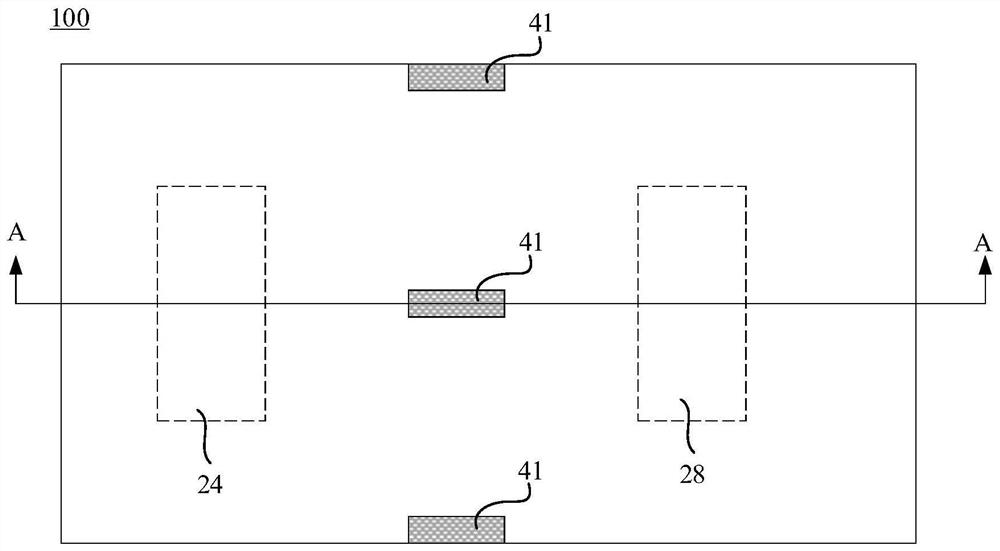
[0075] S130, forming a patterned sacrificial layer on the connection surface, where the sacrificial layer includes at least one first opening;

[0076] S140, forming an isolation layer on a side of the sacrificial layer away from the micro light-emitting diode chip, the isolation layer fills the first opening, and the isolation layer forms a connection structure at the first opening.

[0077] The micro-light emitting element array substrate manufactured by the above method can form a stable connection between the sacrificial layer and the micro light emitting diode chip, and the connection structure can form a stable conn...


PUM


Abstract

The invention discloses a micro light-emitting element array substrate, and a preparation method and a transfer method thereof. The micro light-emitting element array substrate comprises: a substrate; micro light-emitting diode chips, which are distributed on the substrate in an array mode, wherein the surfaces, away from the substrate, of the micro light-emitting diode chips are connecting surfaces; a sacrificial layer, which is arranged on the connecting surface and comprises at least one first opening; an isolation layer, wherein at least a part of the isolation layer is arranged on the side, away from the micro light-emitting diode chips, of the sacrificial layer, the first opening is filled with the isolation layer, the isolation layer forms a connecting structure at the first opening, and the connecting structure is in direct contact with the micro light-emitting diode chips. The micro light-emitting element array substrate provided by the invention can be stably connected with a temporary substrate, and the substrate is easy to strip; and meanwhile, the micro light-emitting diode chips can be conveniently separated from the temporary substrate, so the micro light-emitting diode chips are prevented from being damaged, and the manufacturing yield of a display panel is improved.

Description

technical field [0001] The invention relates to the field of display technology, in particular to a micro-light-emitting element array substrate, a preparation method of the micro-light-emitting element array substrate, and a transfer method of micro-light-emitting diode chips. Background technique [0002] Micro-LED (μLED / Micro-LED) display technology refers to the technology of realizing light-emitting display with high-density integrated tiny light-emitting diode arrays on the substrate as pixels. At present, micro-light-emitting diode technology has gradually become a research hotspot, and the industry expects high-quality micro-light-emitting diode products to enter the market. High-quality micro-LED products will have a profound impact on display products such as LCD (Liquid Crystal Display) / OLED (Organic Light-Emitting Diode Display) already on the market. However, due to the small size of micro-light emitting diodes and the small distance between adjacent micro-ligh...

Claims


Application Information

Patent Timeline
Patent Type & Authority Applications(China)
IPC IPC(8): H01L27/15H01L21/67H01L33/00
CPCH01L21/67144H01L27/156H01L33/0075
Inventor 郭恩卿李庆王程功田文亚
Owner CHENGDU VISTAR OPTEOLECTRONICS CO LTD
Why Eureka
Try Eureka