Solar cell and cell module
A solar cell and electrode technology, applied in electrical components, circuits, photovoltaic power generation, etc., can solve the problems of large power drop and heat generation, and achieve the effects of less power drop, less heat generation, and reduced size of components
- Summary
- Abstract
- Description
- Claims
- Application Information
AI Technical Summary
Problems solved by technology
Method used
Image

Examples
Embodiment 1
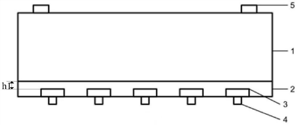
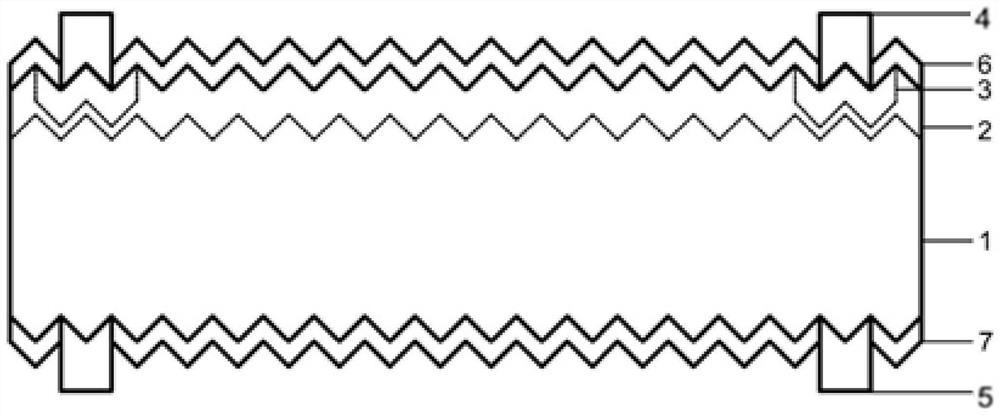
[0047] refer to Figure 4 as shown, Figure 4 A schematic structural view of a fourth solar cell in an embodiment of the present invention is shown. Figure 4 The middle substrate layer 1 is made of n-type single crystal silicon wafer with a doping concentration of 1×10 16 cm -3 , the thickness is 150um. The inversion layer 2 is located on the entire backlight surface of the base layer 1, and is diffused into a p-type layer by using a shallow junction process. The average depth of the inversion layer 2 is 100 nm. A first heavily doped region 3 is provided under the inversion layer 2 by ion implantation or laser technology. The doping concentration of the first heavily doped region 3 is 1×10 18 cm -3 . Along the direction away from the base layer 1, the thickness difference between the inversion layer 2 and the first heavily doped region 3 is 10 nm.
Embodiment 2
[0049] refer to figure 2 As shown, the base layer 1 is made of n-type single crystal silicon wafer with a doping concentration of 1×10 16 cm -3 , the thickness is 150um. Both the light facing surface and the backlighting surface of the base layer 1 are of suede structure.
[0050] The inversion layer 2 is located on the entire light-facing surface of the base layer 1, and is diffused into a p-type layer by using a shallow junction process. The average depth of the inversion layer 2 is 700nm.
[0051] A first heavily doped region 3 is provided in the inversion layer 2 by laser technology. The doping concentration of the first heavily doped region 3 is 1×10 18 cm -3 , along the direction away from the base layer 1, the thickness difference between the inversion layer 2 and the first heavily doped region 3 is 50 nm.
Embodiment 3
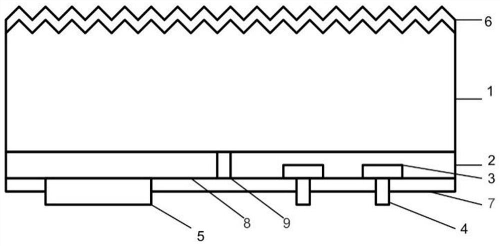
[0053] refer to image 3 As shown, the base layer 1 adopts n-type single crystal silicon wafer, and the doping concentration is 0.5×10 16 cm -3 , with a thickness of 100um. The smooth surface of the base layer 1 is a suede structure, which may have a front surface field.
[0054] The inversion layer 2 is located in a local area of the backlight surface of the base layer 1, and is diffused into a p-type layer by using a shallow junction process. The average depth of the inversion layer 2 is 100nm.
[0055] On the backlight surface of the base layer 1 , except for the rest of the inversion layer 2 , a second heavily doped region 8 is provided. The second heavily doped region 8 is n-type doped, and the doping concentration is higher than that of the base layer 1 . A blocking structure 9 is provided between the second heavily doped region 8 and the inversion layer 2 , and the blocking structure 9 is an insulating gap or a dielectric material.
[0056] A first heavily doped ...
PUM
| Property | Measurement | Unit |
|---|---|---|
| Thickness | aaaaa | aaaaa |
Abstract
Description
Claims
Application Information
 - R&D Engineer
- R&D Manager
- IP Professional
- Industry Leading Data Capabilities
- Powerful AI technology
- Patent DNA Extraction
Browse by: Latest US Patents, China's latest patents, Technical Efficacy Thesaurus, Application Domain, Technology Topic.
© 2024 PatSnap. All rights reserved.Legal|Privacy policy|Modern Slavery Act Transparency Statement|Sitemap