Inverted electroluminescent device, preparation method thereof and display device
A technology of electroluminescence devices and display devices, applied in the fields of electric solid state devices, semiconductor/solid state device manufacturing, electrical components, etc.
- Summary
- Abstract
- Description
- Claims
- Application Information
AI Technical Summary
Problems solved by technology
Method used
Image

Examples
preparation example Construction
[0043] In this embodiment, the preparation method of the inverted electroluminescent device 100 includes the following steps:
[0044] Step S10a, providing a cathode 101 .
[0045] The material of the cathode 101 can be selected from transparent and conductive oxides, such as ITO, AZO, IZO, FTO, IZTO, IGTO and the like. Specifically, taking ITO as an example, the ITO substrate can be directly purchased from the market, or can be prepared by using ITO to form an ITO thin film on a glass substrate. In actual operation, the surface of the obtained ITO substrate is cleaned, dried and then baked at 150° C. for subsequent steps.
[0046] In step S20a , the high molecular polymer is made into a solution, and then coated on the upper surface of the cathode 101 to form the insulating layer 102 .
[0047] In this embodiment, a polymer is dissolved in a common organic solvent (eg, acetone) in the field to make a solution, and then the solution is coated on the upper surface of the cath...
Embodiment 1
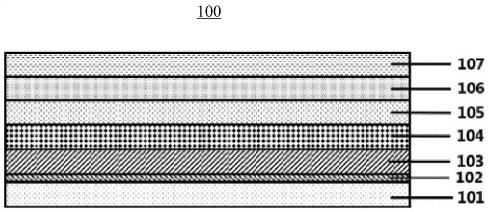
[0060] The structure of the inverted organic light emitting diode in this embodiment is as follows: figure 1 As shown, the OLED includes a cathode 101, an insulating layer 102, an electron transport layer 103, a light emitting layer 104, a hole transport layer 105, a hole injection layer 106, and an anode 107 stacked sequentially from bottom to top, and the material and thickness of each layer Corresponding to ITO / PMMA(3nm) / BPhen(20nm) / Alq 3 (30nm) / NPB(30nm) / MoO 3 (8nm) / Al(100nm).
[0061] (1) The surface of the ITO substrate was ultrasonically cleaned with glass cleaner, pure water, and isopropanol in sequence, and then dried with nitrogen, and then the ITO substrate was baked at 150° C. for 1 hour to serve as the cathode 101 .
[0062] (2) Dissolve the PMMA material (polymethyl methacrylate) in an acetone solvent to prepare a PMMA solution of 1 mg / ml; spin-coat the PMMA solution on the surface of the substrate obtained in step (1), and then place it at 60°C for baking Aft...
Embodiment 2
[0065] The structure of the inverted organic light emitting diode in this embodiment is as follows: figure 1 As shown, the OLED includes a cathode 101, an insulating layer 102, an electron transport layer 103, a light emitting layer 104, a hole transport layer 105, a hole injection layer 106, and an anode 107 stacked sequentially from bottom to top, and the material and thickness of each layer Corresponding to ITO / Al 2 o 3 (2nm) / BPhen(20nm) / Alq 3 (30nm) / NPB(30nm) / MoO 3 (8nm) / Al(100nm).
[0066] (1) The surface of the ITO substrate was ultrasonically cleaned using glass cleaning agent, pure water, and isopropanol in sequence, then blown dry with nitrogen, and then baked the ITO substrate at 150° C. for 1 hour to serve as the cathode 101 .
[0067] (2) Transfer the substrate processed in step (1) to the atomic layer deposition chamber, using trimethylaluminum and water as precursor sources, and prepare Al with a thickness of 2 nm by ALD (atomic layer deposition) process 2 o...
PUM
| Property | Measurement | Unit |
|---|---|---|
| thickness | aaaaa | aaaaa |
| thickness | aaaaa | aaaaa |
| thickness | aaaaa | aaaaa |
Abstract
Description
Claims
Application Information
 - R&D Engineer
- R&D Manager
- IP Professional
- Industry Leading Data Capabilities
- Powerful AI technology
- Patent DNA Extraction
Browse by: Latest US Patents, China's latest patents, Technical Efficacy Thesaurus, Application Domain, Technology Topic.
© 2024 PatSnap. All rights reserved.Legal|Privacy policy|Modern Slavery Act Transparency Statement|Sitemap