Flash memory wear method and device, readable storage medium and electronic equipment
A wear device, flash memory technology, applied in the field of readable storage media and electronic equipment, devices, flash memory wear methods, can solve problems such as low work efficiency
- Summary
- Abstract
- Description
- Claims
- Application Information
AI Technical Summary
Problems solved by technology
Method used
Image
Examples
Embodiment 1
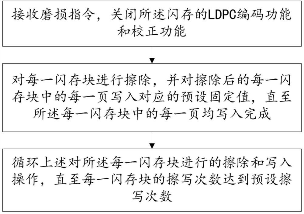
[0060] Please refer to figure 2 , a flash memory wear method comprising the steps of:
[0061] S1. Receive a wear instruction, and turn off the LDPC encoding function and correction function of the flash memory;
[0062] Specifically, in this embodiment, after receiving the wear command, the LDPC function and the scrambler (scrambler) are turned off to prevent the LDPC from generating check data and prevent the scrambler from scrambling when writing data, so as to ensure subsequent Fixed data can be written when flash memory is written;
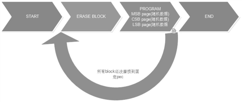
[0063] S2. Erase each flash memory block, and write a corresponding preset fixed value to each page in each flash memory block after erasing, until each page in each flash memory block is written Finish;
[0064] Wherein, each flash memory block is erased and written into a corresponding preset fixed value one by one in a preset order until each flash memory block has been erased and written once;
[0065] Wherein, writing the correspond...
Embodiment 2
[0078] The difference between this embodiment and Embodiment 1 is that how to determine the preset fixed value is specifically defined:
[0079] Wherein, the preset fixed value is the level value of each bit of the corresponding memory cell when the threshold voltage applied to the flash memory is maximum;
[0080] Among them, in this example, please refer to Figure 7 , usually when writing, no matter what data is written, after the write operation is scrambled by the scrambler module at the host control end, the 0 and 1 values of each page in the flash memory block will be evenly distributed, so that The memory cells of the entire page are evenly distributed among Figure 7 Among the 8 states of Figure 7 The abscissa in the middle is the read threshold voltage Vr, and the ordinate is the number of cells. The more you go to the right, the greater the voltage, and the greater the voltage applied during writing, the greater the wear on the memory cell. Figure 7 The 8 sta...
Embodiment 3
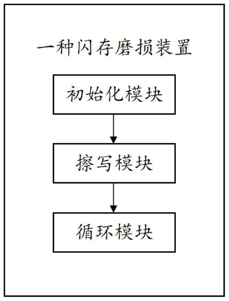
[0087] Please refer to image 3 , a flash wear device comprising:
[0088] The initialization module is used to receive the wear instruction, and close the LDPC encoding function and correction function of the flash memory;
[0089] The erasing and writing module is used to erase each flash memory block, and writes a corresponding preset fixed value to each page in each flash memory block after erasing, until each flash memory block in each All pages are written;
[0090] The cycle module is used to cycle the above-mentioned erasing and writing operations on each flash memory block until the number of times of erasing and writing of each flash memory block reaches a preset number of times of erasing and writing.
PUM
 Abstract
Description
Claims
Application Information
 - R&D
- Intellectual Property
- Life Sciences
- Materials
- Tech Scout
- Unparalleled Data Quality
- Higher Quality Content
- 60% Fewer Hallucinations
Browse by: Latest US Patents, China's latest patents, Technical Efficacy Thesaurus, Application Domain, Technology Topic, Popular Technical Reports.
© 2025 PatSnap. All rights reserved.Legal|Privacy policy|Modern Slavery Act Transparency Statement|Sitemap|About US| Contact US: help@patsnap.com


