Check patentability & draft patents in minutes with Patsnap Eureka AI!

Layout wiring method based on multiple masks

A wiring method and mask technology, which can be used in instrumentation, computing, electrical and digital data processing, etc., and can solve problems such as huge workload and cost.

Active Publication Date: 2021-05-18
北京华大九天科技股份有限公司
View PDF17 Cites 1 Cited by
  • Summary
  • Abstract
  • Description
  • Claims
  • Application Information

AI Technical Summary

Problems solved by technology

[0004] The existing method to solve graphic distortion is to perform layout decomposition and coloring after wiring (post-wiring coloring), but as the design scale and complexity increase, there may be more conflicts in layout decomposition, or there may be no solution. It needs to be solved by modifying the design, facing huge workload and cost

Method used


Image

  • Layout wiring method based on multiple masks
  • Layout wiring method based on multiple masks
  • Layout wiring method based on multiple masks

Examples


Embodiment 1

[0054]figure 1 In accordance with the multi-mask version of the multi-mask version of the multi-mask version, the reference will be referenced below.figure 1 The multi-mask-based layout method of the present invention is described in detail.

[0055]First, in step 101, the wiring resource is initialized.

[0056]In the embodiment of the present invention, the initialization of the wiring resources, including, process data (Design Rule), the basic data such as wiring layer, via holes, etc., the desired wiring mesh (NET) and wiring graphics read , The initialization of the wiring window, the initialization of the wiring mesh, the initialization of the wiring resources required during the algorithm expansion process.

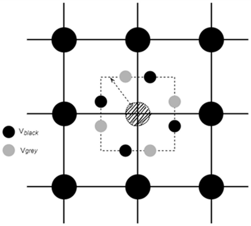
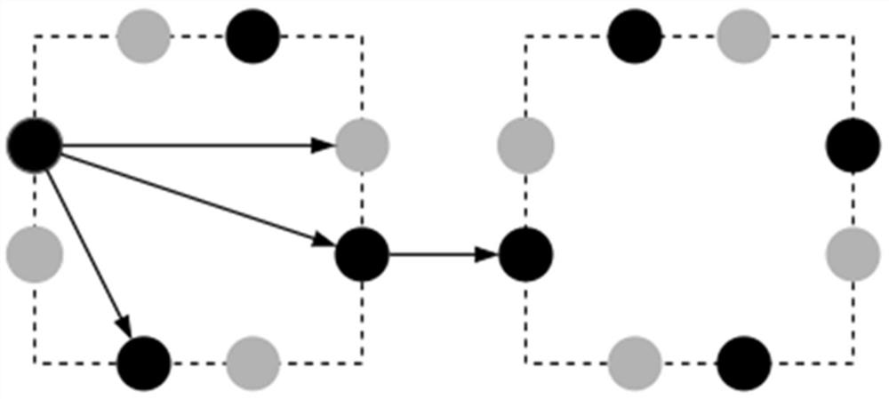
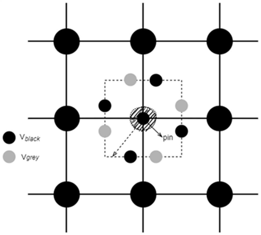
[0057]At step 102, the grid node is modeled to obtain the extended grid of the wiring grid.

[0058]In the embodiment of the present invention, the grid node is modeled, and a mesh node is abstracted to have a plurality of sub-nodes, which constitute a wiring grid of the wiring grid...


PUM


Abstract

The invention discloses a layout wiring method based on multiple masks. The layout wiring method comprises the following steps: initializing wiring resources; constructing a node graph model to obtain an expansion grid of the wiring grid; and carrying out shortest path search and expansion on the expansion grid, and carrying out network wiring. According to the layout wiring method based on the multiple masks, in the detailed wiring process of a super-large-scale integrated circuit, sutures and conflicts generated in the wiring process of an existing wiring technology are reduced, the wiring result is optimized, and the manufacturability of the super-large-scale integrated circuit is enhanced.

Description

Technical field[0001]The present invention relates to the field of integrated circuit detailed wiring design, and more particularly to a large-scale integrated circuit (VLSI) layout method.Background technique[0002]In recent years, with the rapid development of science and technology, people's cognition and emphasis on integrated circuits are gradually improved, while the chip manufacturing in the integrated circuit has also entered the nano-era with the development of the times. . The integration of the chip is gradually improved, more and more circuit components needed on a piece of chip, plus the limitations of storage space and the limitations of the packaging technology process, and the ultra-large scale integrated circuit (Very Large ScaleInstegration, hereinafter referred to as VLSI) The design puts forward higher requirements.[0003]The wiring is the most time consuming in large-scale integrated circuit design, and he is also an extremely important impact on the power consump...

Claims


Application Information

Patent Timeline
IPC IPC(8): G06F30/394G06F30/398
CPCG06F30/394G06F30/398
Inventor 陈婧张亚东蔡小五谢光益李起宏陆涛涛
Owner 北京华大九天科技股份有限公司
Features
  • R&D
  • Intellectual Property
  • Life Sciences
  • Materials
  • Tech Scout
  • Unparalleled Data Quality
  • Higher Quality Content
  • 60% Fewer Hallucinations
Learn More