Check patentability & draft patents in minutes with Patsnap Eureka AI!

Micromechanical device and method for manufacturing a micromechanical device

a micromechanical and manufacturing method technology, applied in the field of micromechanical devices, can solve the problems of limited degree, no fuses at all or local fuses of the substrate, etc., and achieve the effects of good heat conductivity, favorable geometry, and less stress on the substra

Active Publication Date: 2022-03-01
ROBERT BOSCH GMBH
View PDF13 Cites 0 Cited by
  • Summary
  • Abstract
  • Description
  • Claims
  • Application Information

AI Technical Summary

Benefits of technology

The present invention provides a way to create an additional access channel using a DRIE trench, which allows for a high aspect ratio and minimal space usage. This design also enables a self-adjusting effect of the laser relative to the structure of the functional layer, reducing manufacturing sensitivity and improving reliability.

Problems solved by technology

The result that may be achieved by this is that the functional layer fuses, but the substrate does not fuse at all or fuses locally only to a very limited degree due to the comparatively better heat conductivity, to the more favorable geometry and due to the chronological dynamics.

Method used


Image

  • Micromechanical device and method for manufacturing a micromechanical device
  • Micromechanical device and method for manufacturing a micromechanical device
  • Micromechanical device and method for manufacturing a micromechanical device

Examples


Embodiment Construction

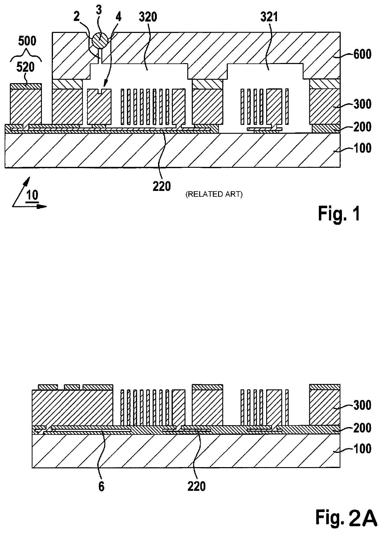
[0025]FIG. 1 shows a micromechanical device in the related art. The device includes a silicon substrate 100 with an overlying oxide layer 200 and with a micromechanical functional layer 300 lying above same, which extend in parallel to a main extension plane 10. Oxide layer 200 is constructed of multiple layers and contains at least one electrical wiring plane 220, which contacts the micromechanical device. Two cavities 320, 321 are formed in micromechanical functional layer 300 and in oxide layer 200. The cavities are closed off by a cap 600. A vertical access channel 2 is introduced through cap 600 into cavity 320. Situated opposite access channel 2 is a beam trap 4. In addition, micromechanical functional structures are situated in cavity 320. Access channel 2 is sealed with a laser melt seal 3. A bonding pad area 500, which is formed in functional layer 300, is situated next to cap 600 as viewed perpendicularly to main extension plane 10. Bonding pad area 520 includes bonding pa...


PUM

PropertyMeasurementUnit
areaaaaaaaaaaa
thicknessaaaaaaaaaa
thermal conductivityaaaaaaaaaa

Abstract

A micromechanical device that includes a silicon substrate with an overlying oxide layer and with a micromechanical functional layer lying above same, which extend in parallel to a main extension plane, a cavity being formed at least in the micromechanical functional layer and in the oxide layer. An access channel is formed in the oxide layer and / or in the micromechanical functional layer which, starting from the cavity, extends in parallel to the main extension plane and in the process extends in a projection direction, as viewed perpendicularly to the main extension plane, all the way into an access area outside the cavity. A method for manufacturing a micromechanical device is also described.

Description

CROSS REFERENCE[0001]The present application claims the benefit under 35 U.S.C. § 119 of German Patent Application No. DE 102018222804.3 filed on Dec. 21, 2018, which is expressly incorporated herein by reference in its entirety.FIELD[0002]The present invention is directed to a micromechanical device that includes a silicon substrate with an overlying oxide layer and with a micromechanical functional layer lying above same, which extend in parallel to a main extension plane, a cavity being formed at least in the micromechanical functional layer and in the oxide layer.BACKGROUND INFORMATION[0003]Silicon-micromechanical-based sensors are employed in the automotive industry and in entertainment electronics for measuring acceleration, rotation rate, pressure, magnetic field and other parameters. The advantage of silicon wafer technology is that these sensors are fabricated on a mass production scale. The major trends in the ongoing development in the field of entertainment electronics a...

Claims


Application Information

Patent Timeline
Patent Type & Authority Patents(United States)
IPC IPC(8): B81B3/00B81C1/00
CPCB81C1/00119B81B3/0097B81B2203/0315B81B2207/098B81C2201/0132B81C2203/0118B81C2203/0172B81B7/0041B81B7/0045B81C1/00325B81C1/00293B81B7/02B81B7/0061
Inventor GRAF, ECKHARDRUMPF, HOLGERFREY, JENSREINMUTH, JOCHENRITZAU, KURT-ULRICHBREITLING, ACHIM
Owner ROBERT BOSCH GMBH
Features
  • R&D
  • Intellectual Property
  • Life Sciences
  • Materials
  • Tech Scout
  • Unparalleled Data Quality
  • Higher Quality Content
  • 60% Fewer Hallucinations
Learn More