Chip packaging structure and preparation method of chip packaging structure

A chip packaging structure and chip packaging technology, applied in semiconductor/solid-state device manufacturing, electrical components, electric solid-state devices, etc., can solve problems such as poor heat dissipation

Active Publication Date: 2021-05-18
FOREHOPE ELECTRONICS NINGBO CO LTD
View PDF9 Cites 12 Cited by
  • Summary
  • Abstract
  • Description
  • Claims
  • Application Information

AI Technical Summary

Problems solved by technology

With the traditional stacked structure, as the number of memory chips increases, the size of the product increases, and the size of the plastic packaging layer increases, resulting in poorer heat dissipation performance

Method used


Image

  • Chip packaging structure and preparation method of chip packaging structure
  • Chip packaging structure and preparation method of chip packaging structure
  • Chip packaging structure and preparation method of chip packaging structure

Examples


no. 1 example

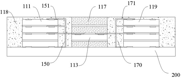
[0036] see figure 1 The embodiment of the present invention provides a chip packaging structure 100 with good heat dissipation effect. At the same time, through the stacked structure of the first memory chip 111, multiple chips can be stacked, which increases the number of stacks and ensures good heat dissipation effect.

[0037] The chip packaging structure 100 provided in this embodiment includes a dielectric layer 130 and a chip packaging module 110 disposed on the dielectric layer 130, wherein the chip packaging module 110 can be prepared in advance, and a dielectric layer is formed on the bottom of the chip packaging module 110 after the chip packaging module 110 is prepared. layer 130, or attach the chip packaging module 110 on the dielectric layer 130 prepared in advance.

[0038] The chip packaging module 110 includes a logic chip 113, a plurality of first memory chips 111, at least one first heat dissipation block 115, at least one second heat dissipation block 117 and ...

no. 2 example

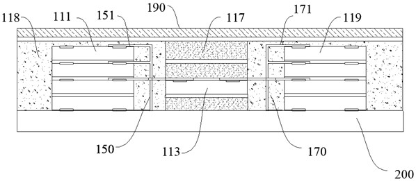
[0057] see figure 2 , this embodiment provides a chip packaging structure 100, the basic structure and principle and the technical effect produced are the same as those of the first embodiment, for a brief description, the parts not mentioned in this embodiment can refer to the first embodiment corresponding content.

[0058]In this embodiment, the chip packaging structure 100 includes a dielectric layer 130 and a chip packaging module 110 disposed on the dielectric layer 130, wherein the chip packaging module 110 can be prepared in advance, and formed on the bottom of the chip packaging module 110 after the chip packaging module 110 is prepared. dielectric layer 130 , or attach the chip packaging module 110 on the dielectric layer 130 prepared in advance. The chip packaging module 110 includes a plurality of first memory chips 111, a plurality of second memory chips 119, a logic chip 113, at least one first heat dissipation block 115, at least one second heat dissipation bl...

no. 3 example

[0062] This embodiment provides a method for manufacturing a chip packaging structure 100, which is used to prepare the chip packaging structure 100 provided in the first embodiment or the second embodiment.

[0063] The preparation method includes:

[0064] S1 : Prepare the chip packaging module 110 on the carrier 200 .

[0065] Specifically, use the carrier 200 to prepare the chip packaging module 110, mold the chip packaging module 110 on the carrier 200, remove the carrier 200 at last, form the dielectric layer 130 on the bottom side of the chip packaging module 110 after molding, or package the chip The module 110 is mounted on the pre-prepared dielectric layer 130 . The carrier 200 can be made of glass, silicon oxide, metal and other materials, and the chip packaging module 110 can be prepared by using the carrier 200, which can eliminate the warping problem during the manufacturing process and ensure the structural stability of the chip packaging module 110.

[0066] ...


PUM


Abstract

The embodiment of the invention provides a chip packaging structure and a preparation method of the chip packaging structure, and relates to the technical field of chip packaging, and the chip packaging structure comprises a dielectric layer and a chip packaging module arranged on the dielectric layer. The chip packaging module comprises a plurality of first storage chips, a logic chip, at least one first heat dissipation block, at least one second heat dissipation block and a plastic packaging layer. The first storage chips are arranged on a dielectric layer in a stacked mode, the first heat dissipation blocks are arranged on the dielectric layer, the logic chip is arranged on the first heat dissipation blocks, the second heat dissipation blocks are arranged on the logic chip, and extend to the surface of the plastic packaging layer. Compared with the prior art, by arranging the first heat dissipation block and the second heat dissipation block, the good heat dissipation effect of the logic chip can be guaranteed, meanwhile, through the stacking structure of the first storage chip, stacking of multiple chips is achieved, the stacking number is increased, and meanwhile the good heat dissipation effect is guaranteed.

Description

technical field [0001] The invention relates to the technical field of chip packaging, in particular to a chip packaging structure and a method for preparing the chip packaging structure. Background technique [0002] With the rapid development of the semiconductor industry, the miniaturization of electronic products is becoming thinner and thinner to meet the needs of users and the product performance and memory are getting higher and higher. Therefore, the semiconductor packaging structure adopts multiple chip stacking (Stack-Die or FOW film sticking Package) technology, which stacks two or more chips in a single package structure to reduce product package volume and improve product performance. This kind of stacked product (memory card / memory card) usually has two types of chips, memory storage chip and control chip, which are packaged in the same substrate unit by stacking. The performance of the memory card is limited by the number of memory chips and the size of the s...

Claims


Application Information

Patent Timeline
Patent Type & Authority Applications(China)
IPC IPC(8): H01L25/18H01L23/367H01L23/485H01L23/482H01L21/50H01L21/60
CPCH01L21/50H01L23/367H01L23/4824H01L23/485H01L24/03H01L25/18H01L2224/02331H01L2224/02333H01L2224/02381
Inventor 包宇君何正鸿钟磊
Owner FOREHOPE ELECTRONICS NINGBO CO LTD
Why Eureka
Try Eureka