MOSFET device capable of improving anti-static capability, and manufacturing method

An anti-static and manufacturing method technology, applied in semiconductor/solid-state device manufacturing, electrical components, semiconductor devices, etc., can solve the problems of complex manufacturing process and high cost

Pending Publication Date: 2021-05-18
捷捷微电(无锡)科技有限公司
View PDF0 Cites 0 Cited by
  • Summary
  • Abstract
  • Description
  • Claims
  • Application Information

AI Technical Summary

Problems solved by technology

[0013] The process of this method requires 6 times of ph...

Method used


Image

  • MOSFET device capable of improving anti-static capability, and manufacturing method
  • MOSFET device capable of improving anti-static capability, and manufacturing method
  • MOSFET device capable of improving anti-static capability, and manufacturing method

Examples


Embodiment Construction

[0062] The present invention will be further described below in conjunction with specific examples.

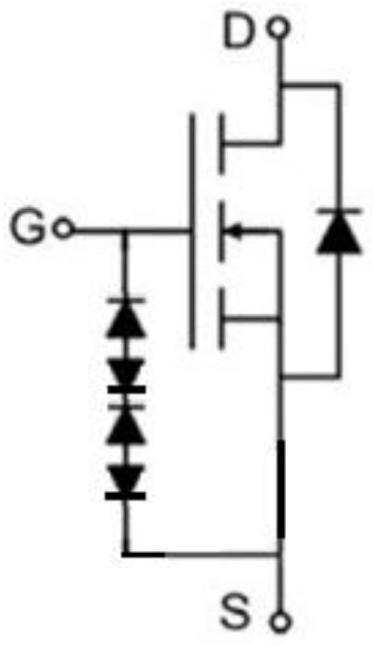
[0063] A MOSFET device with improved antistatic capability in the following embodiment 1, taking an N-type trench gate MOSFET as an example, the first conductivity type is N-type, and the second conductivity type is P-type;

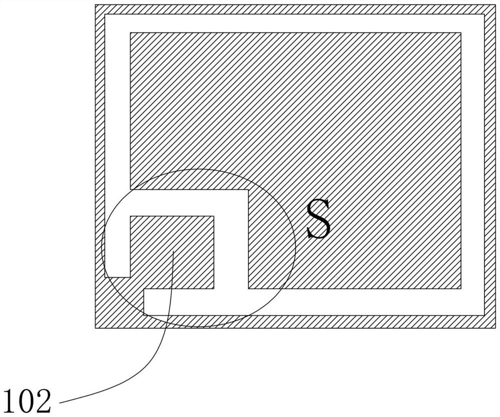
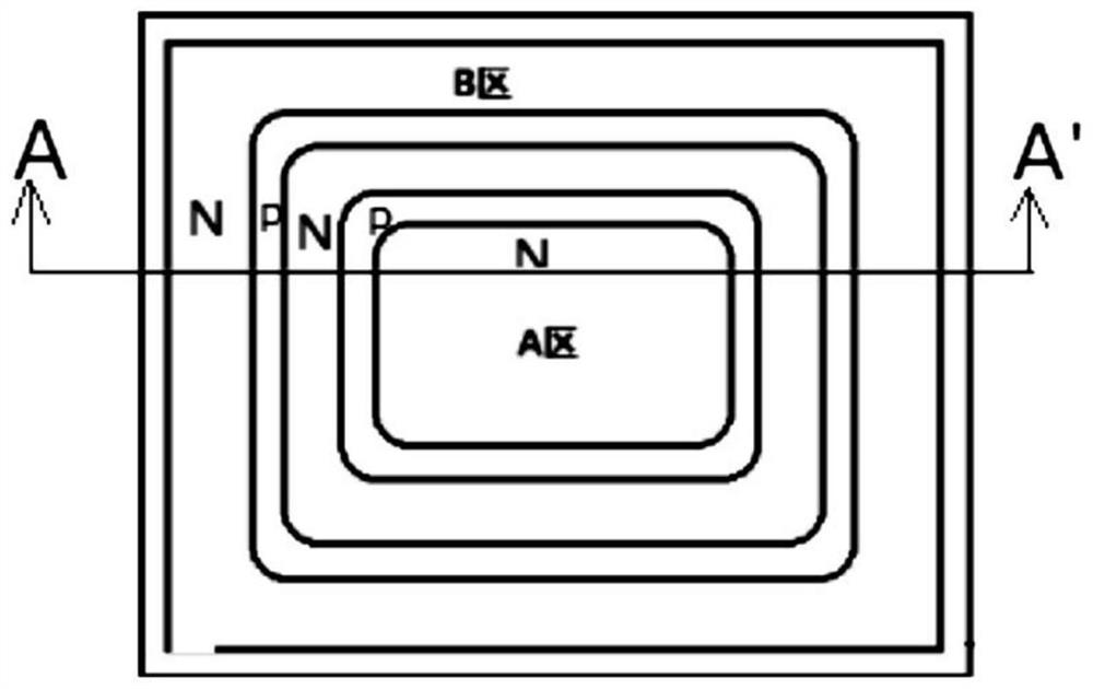
[0064] as attached Figure 5 As shown, a MOSFET device with improved antistatic capability includes a gate metal 10 used to lead out the gate and a source metal 9 used to lead out the source, and the gate metal 10 and the source metal 9 are provided with An ESD protection structure, the ESD protection structure includes a plurality of ESD protection trenches 3, the plurality of ESD protection trenches 3 are arranged in parallel around the gate PAD region 102, the gate is connected in series with a gate resistor Rg, The gate resistor Rg includes a plurality of gate resistor trenches 4, and the plurality of gate resistor trenches 4 are arranged between the...


PUM


Abstract

The invention relates to an MOSFET device capable of improving the anti-static capability, and a manufacturing method thereof. The MOSFET device comprises gate metal for leading out a gate and source metal for leading out a source, an ESD protection structure is arranged between the gate metal and the source metal, the ESD protection structure comprises a plurality of ESD protection grooves, the plurality of ESD protection grooves are arranged in parallel around a gate PAD region, the gate is connected with a plurality of gate resistors Rg in series, the gate resistors Rg comprise gate resistor grooves, and the gate resistor grooves are arranged between the active region and the terminal protection region; and on the basis of an existing device with an ESD protection structure, the gate resistors Rg are connected to the gate in series, when the grid is impacted by strong static electricity, the Rg resistors enable the static electricity to flow to a polycrystalline silicon diode loop, a thin gate oxide structure of an MOS is effectively protected, and an original conventional diode protection loop (PN junction pair) plays a greater protection role, so the anti-ESD capability limit of the device is improved, and the reliability of the device is improved.

Description

technical field [0001] The invention relates to a power semiconductor device, in particular to a MOSFET device and a manufacturing method with improved antistatic capability, belonging to the technical field of power semiconductor devices. Background technique [0002] Power MOSFET devices play an important role in the modern electronics industry. With the expansion of the application range of devices, more and more people have higher requirements for the antistatic ability of devices. It can be seen from the device structure of MOSFET that there is only a thin layer of oxide layer separating the gate and source of MOSFET. This oxide layer is generally within 100nm. When the MOS device has no special structure protection, its ESD resistance is very low. , generally within 500V, in a relatively dry environment, it is far lower than the static value generated by the common human body, which can easily cause permanent damage to the device. [0003] In order to make MOSFET devi...

Claims


Application Information

Patent Timeline
IPC IPC(8): H01L29/78H01L29/06H01L21/336
CPCH01L29/0619H01L29/66712H01L29/7802H01L29/7805
Inventor 殷允超刘锋费国芬
Owner 捷捷微电(无锡)科技有限公司
Why Eureka
Try Eureka