Array substrate and display panel

An array substrate and drain technology, applied in instruments, semiconductor devices, optics, etc., can solve problems such as data line short circuit, display panel bright spots or vertical line defects, and achieve the effect of reducing area and improving display quality

Inactive Publication Date: 2021-05-25
SHENZHEN CHINA STAR OPTOELECTRONICS TECH CO LTD
View PDF5 Cites 1 Cited by
  • Summary
  • Abstract
  • Description
  • Claims
  • Application Information

AI Technical Summary

Problems solved by technology

[0005] The embodiment of the present application provides an array substrate and a display panel, aiming to improve the problem that the drain and the data line in the existing display panel are prone to short circuit, resulting in bright spots or poor vertical lines on the display panel.

Method used


Image

  • Array substrate and display panel
  • Array substrate and display panel
  • Array substrate and display panel

Examples


Embodiment Construction

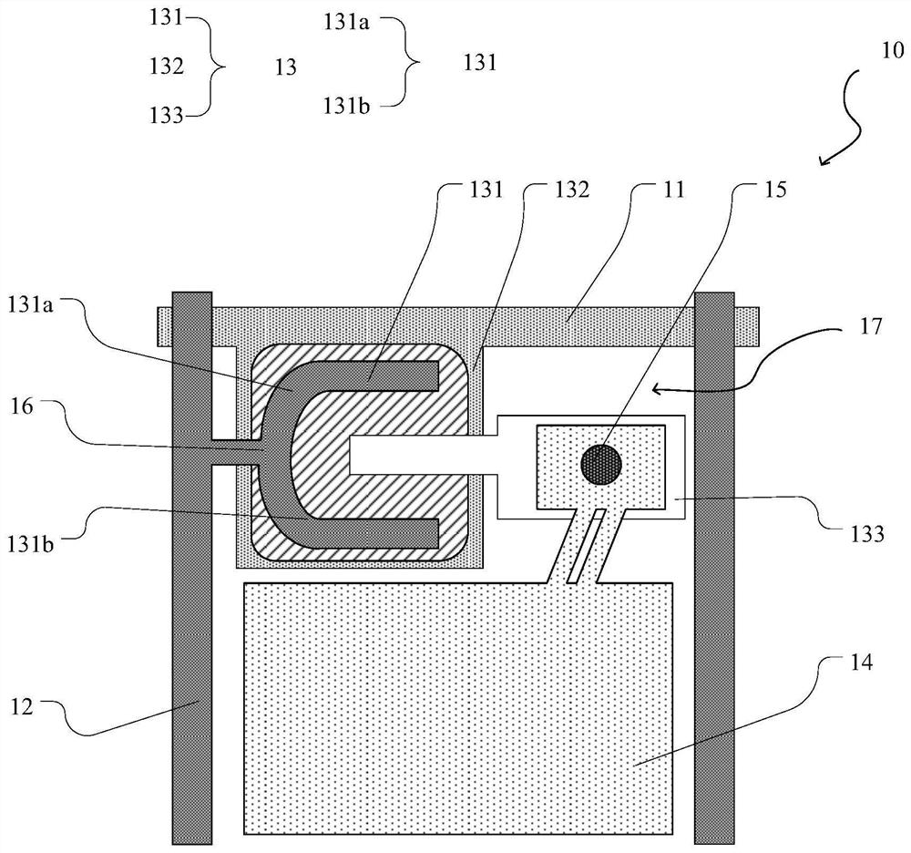
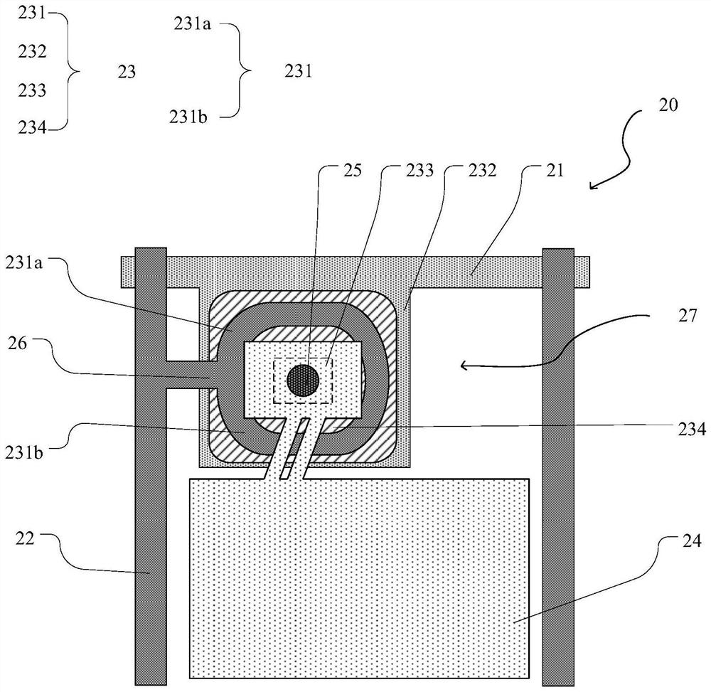
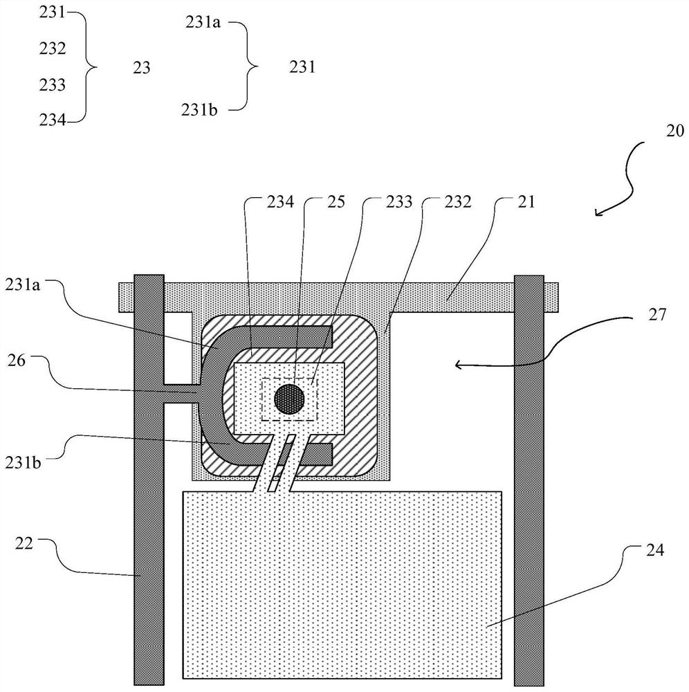
[0032] The technical solutions in the embodiments of the present application will be clearly and completely described below in conjunction with the drawings in the embodiments of the present application. Apparently, the described embodiments are only some of the embodiments of this application, not all of them. Based on the embodiments in this application, all other embodiments obtained by those skilled in the art without making creative efforts belong to the scope of protection of this application.

[0033] In the description of the present application, it should be understood that the terms "center", "longitudinal", "transverse", "length", "width", "thickness", "upper", "lower", "front", " Orientation indicated by rear, left, right, vertical, horizontal, top, bottom, inside, outside, clockwise, counterclockwise, etc. The positional relationship is based on the orientation or positional relationship shown in the drawings, which is only for the convenience of describing the a...


PUM


Abstract

The invention discloses an array substrate and a display panel. The array substrate comprises a plurality of scanning lines, a plurality of data lines and a plurality of sub-pixel units; each sub-pixel unit comprises a thin film transistor and a pixel electrode, and each thin film transistor comprises a grid electrode connected with the corresponding scanning line, a source electrode connected with the corresponding data line and a drain electrode connected with the corresponding pixel electrode; and in the direction parallel to the plane of the array substrate, the source electrode comprises two branch parts located in the sub-pixel units, the drain electrode is connected with the pixel electrode through a connecting hole, and the drain electrode and the connecting hole are arranged in the range defined by the two branch parts. According to the invention, the drain electrode and the connecting hole are arranged in the range defined by the two branch parts of the source electrode, so that the area occupied by the drain electrode is reduced, and the problem of bright spots or poor vertical line shape of a display panel caused by short circuit of the drain electrode and the data lines is avoided.

Description

technical field [0001] The present application relates to the field of display technology, and in particular to an array substrate and a display panel. Background technique [0002] Liquid crystal display panels are widely used due to their advantages such as wide viewing angle, high brightness, high contrast ratio, low power consumption, and light and thin volume. Among them, the active thin film transistor display panel (Thin Film Transistor-LCD, TFT-LCD) has been rapidly developed and widely used in recent years. Most of the liquid crystal display panels currently on the market are backlight liquid crystal display panels, which include a liquid crystal display panel and a backlight module. Generally, a liquid crystal display panel consists of a color filter substrate (Color Filter, CF), an array substrate (Thin Film Transistor Array Substrate, TFT Array Substrate), a liquid crystal (Liquid Crystal, LC) sandwiched between the color filter substrate and the array substrate...

Claims


Application Information

Patent Timeline
Patent Type & Authority Applications(China)
IPC IPC(8): G02F1/1362G02F1/1368H01L27/12
CPCG02F1/1362G02F1/136227G02F1/1368H01L27/1214H01L29/41733G02F1/136286H01L27/124
Inventor 杨立涛欧阳幸
Owner SHENZHEN CHINA STAR OPTOELECTRONICS TECH CO LTD
Why Eureka
Try Eureka