Semiconductor test data processing method and device

A technology for testing data and processing methods, applied in electrical digital data processing, special data processing applications, digital data information retrieval, etc. Simplified follow-up operations, less demanding effects

Active Publication Date: 2021-06-01
SEMITRONIX
View PDF14 Cites 2 Cited by
  • Summary
  • Abstract
  • Description
  • Claims
  • Application Information

AI Technical Summary

Problems solved by technology

Therefore, even if an effective distributed computing platform is built, a large number of servers are needed to build a platform data analysis platform if one wants to quickly obtain calculation results. In addition, for the sake of security and data confidentiality, we cannot rely entirely on building a data analysis platform to process the data involved in semiconductor testing.

Method used


Image

  • Semiconductor test data processing method and device
  • Semiconductor test data processing method and device
  • Semiconductor test data processing method and device

Examples


Embodiment 1

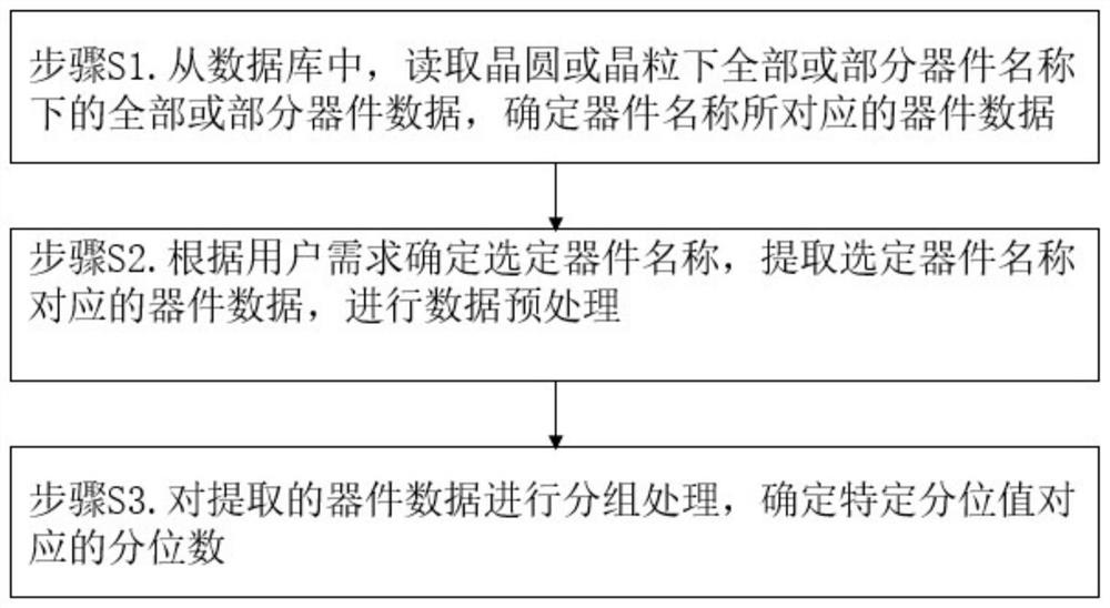
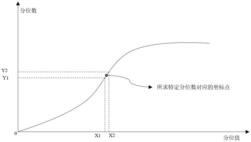
[0027] Such as figure 1 shown, combined with reference figure 2 , in Embodiment 1 of the present invention, the semiconductor test data processing method specifically includes the following steps: Step S1. From the database, read all or part of the test data under the name of all or part of the device under the wafer or grain, and determine the device The test data corresponding to the name; Step S2. Determine the selected device name according to user needs, and extract the test data corresponding to the selected device name; Step S3. Group the extracted test data, and determine the quantile corresponding to the specific quantile value number; including: custom grouping rules, which divide the test data into several groups. Determine the group number of the group it is in and the next group number of the group it is in according to the specific quantile value; Quantile Value Corresponding to Minimum Calculates the quantile value corresponding to a specific quantile value. ...


PUM


Abstract

The invention provides a semiconductor test data processing method, which comprises the following steps of: reading test data with the same device name under different wafers or crystal grains in batches from a database, and determining the test data corresponding to the device name; determining a selected device name according to a user demand, extracting test data corresponding to the selected device name, and preprocessing the test data; and grouping the extracted test data, determining a grouping number based on a specific quantile, and obtaining a quantile corresponding to the specific quantile based on the minimum value of the group corresponding to the adjacent grouping number and the corresponding quantile thereof. Effective quantile calculation and data statistics can be carried out under limited resource configuration, the analysis complexity is simplified, and the efficiency is high. The invention also provides a semiconductor data processing device, which can realize the data processing method provided by the invention, has corresponding advantages, can better realize accurate calculation of quantiles, and is beneficial to improvement of production efficiency.

Description

technical field [0001] The invention belongs to the technical field of data processing and analysis, and in particular relates to a data processing method and a data processing device involved in semiconductor testing. Background technique [0002] With the continuous improvement of semiconductor process technology and the improvement of testing capabilities, both design companies and production foundries have a large amount of data related to semiconductor testing that needs to be processed and analyzed, the most prominent of which is testing during wafer testing. The number is increasing, and the test data that needs to be analyzed and processed is getting larger and larger. When a large amount of test data pours into the data warehouse, data analysts face such a huge test data, how to perform fast and effective processing and analysis, especially how to perform effective quantile calculation and data statistics on the grouped data, become increasingly urgent. For exampl...

Claims


Application Information

Patent Timeline
Patent Type & Authority Applications(China)
IPC IPC(8): G06F16/245G06F16/2455G06F16/2458
CPCG06F16/245G06F16/24556G06F16/2462G06F16/24568Y02P90/30
Inventor 陈小川邵康鹏
Owner SEMITRONIX
Why Eureka
Try Eureka