Deep ultraviolet AlGaN-based light emitting diode with coupled quantum well structure
A technology for coupling quantum wells and light-emitting diodes, applied in electrical components, circuits, semiconductor devices, etc., can solve problems such as low luminous efficiency, achieve the effects of suppressing efficiency decline, reducing Auger recombination rate, and increasing total spontaneous emission recombination rate Effect
- Summary
- Abstract
- Description
- Claims
- Application Information
AI Technical Summary
Problems solved by technology
Method used
Image
Examples
Embodiment 1
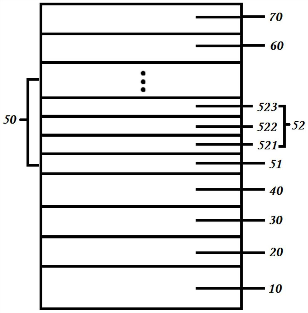
[0017] This embodiment discloses a deep-ultraviolet AlGaN-based light-emitting diode with a coupled quantum well structure. By replacing the traditional well layer with a coupled well layer, the energy band structure of the quantum well is adjusted, and the radiation recombination region of electrons and holes in the well layer is expanded, thereby reducing Auger recombination rate, increase the total spontaneous emission recombination rate, improve the internal quantum efficiency of LED devices, and suppress the effect of device efficiency drop.
[0018] The embodiment of the present invention has an ultraviolet nitride light-emitting diode with a coupled quantum well structure, such as figure 1 As shown, it includes substrate 10 , buffer layer 20 , superlattice layer 30 , n-type semiconductor layer 40 , multiple quantum well structure 50 , p-type semiconductor layer 60 , and p-type ohmic contact layer 70 from bottom to top. Among them, the multi-quantum well structure 50 is ...
Embodiment 2
[0029] This embodiment discloses a deep-ultraviolet AlGaN-based light-emitting diode with a coupled quantum well structure. The difference from Embodiment 1 is that the potential well layer 52 is composed of five layers, which are Al from bottom to top. x Ga 1-x N well layer 521, Al y Ga 1-y N isolation layer 522, Al x Ga 1-x N well layer 523 composition, Al y Ga 1-y N isolation layer 524, Al x Ga 1-x The N-well layer 525 is constituted as Figure 5 shown.
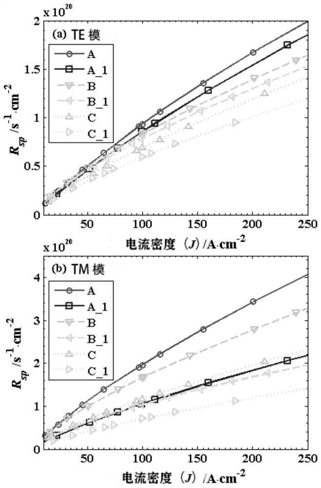
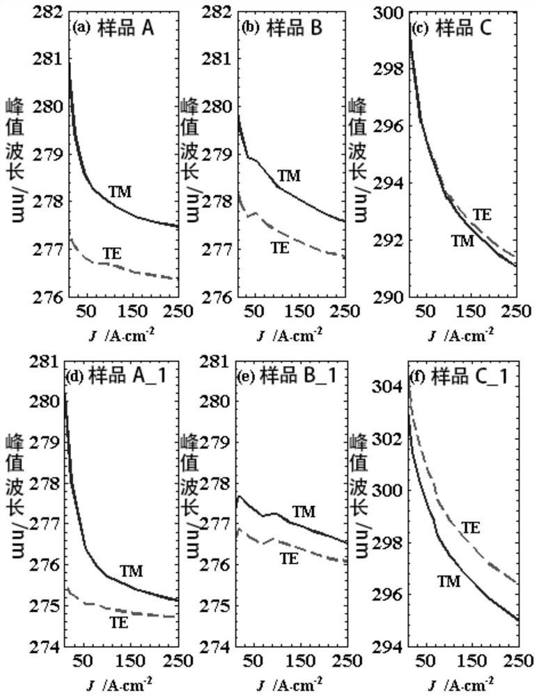
[0030] Figure 6 is the internal quantum efficiency of the coupled quantum well structure (sample XA) and the traditional quantum well structure (sample B and sample C) with potential well layers having a 5-layer structure. The n-type semiconductor layer of sample XA is n-type Al 0.55 Ga 0.45 N material; barrier layer is 8nm thick Al 0.5 Ga 0.5 N; the coupling well layer is sequentially 1 nm thick Al 0.35 Ga 0.65 N, 2nm thick Al 0.5 Ga 0.5 N, 1 nm thick Al 0.35 Ga 0.65 N, 2nm thick Al 0.5 Ga 0.5 N, 1 ...
PUM
| Property | Measurement | Unit |
|---|---|---|
| Luminous wavelength | aaaaa | aaaaa |
| Thickness | aaaaa | aaaaa |
| Thickness | aaaaa | aaaaa |
Abstract
Description
Claims
Application Information


