Storage and calculation integrated operation method and application of self-rectification memristor circuit
An operation method and memristor technology, applied in the field of microelectronics, to achieve the effect of convenient operation, few components and operation steps, and high logic completeness.
- Summary
- Abstract
- Description
- Claims
- Application Information
AI Technical Summary
Problems solved by technology
Method used
Image
Examples
Embodiment 1
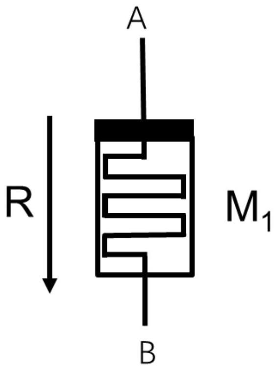
[0084] In order to facilitate the understanding of the implementation process of this scheme, the logic flow of realizing the four-bit square root function based on the self-rectifying memristor array is introduced below; the specific operation steps of realizing the four-bit square root function logic function based on the self-rectifying memristor array are as follows, A total of three self-rectifying memristors are required, denoted as M 1 , M 2 and M 3 ;
[0085]
[0086] f 2 =F 2 (a 3 ,1,a 2 ,1)
[0087] r 1 =a 3 +a 2 =F 3 (a 3 ,0,a 2 ,1)
[0088]
[0089]
[0090] Step 1: put 1, a 2 , 0, 1 are brought into the self-rectifying memristor M 1 In the operation, that is, for M 1 The positive voltage is applied to the upper electrode, and the pressure applied to the lower electrode is the same as a 2 related, a 2 is 1, apply a forward high voltage V s ;a 2 is 0, applying 0 bias; the initial resistance of the self-rectifying memristor is set to hi...
Embodiment 2
[0104] In order to facilitate the understanding of the program implementation process, Figure 10 The flow of implementing NAND logic based on the self-rectifying memristor circuit provided for the embodiment of the present invention, the specific operation steps for implementing the NAND logic function based on the self-rectifying memristor array are as follows:
[0105] The first step: the input signal P and Q 0 Write them into the self-rectifying memristors P and Q for calculation, and the output result is recorded as Q 1 ;
[0106] Step 2: Write the output result of the first step into the self-rectifying memristor P for calculation, and the output result is recorded as Q 2 ;
[0107] Step 3: Write the output result of the second step into the self-rectifying memristor P, and write "1" into the self-rectifying memristor Q for operation, and the output result is recorded as Q 3 ; That is, to realize the input P NAND Q 0 →Q 3 logic function;
[0108] So far, two non-v...
PUM
 Abstract
Description
Claims
Application Information


