A semiconductor wastewater defluorination treatment device

A processing device and semiconductor technology, applied in water/sewage treatment, adsorbed water/sewage treatment, water/sludge/sewage treatment, etc., can solve the problems of reduced work efficiency, inability to meet processing requirements, and inconvenient operation, etc. To achieve the effect of improving the effect and improving the efficiency of wastewater treatment

Active Publication Date: 2021-09-28
深圳市粤昆仑环保实业有限公司
View PDF4 Cites 0 Cited by
  • Summary
  • Abstract
  • Description
  • Claims
  • Application Information

AI Technical Summary

Problems solved by technology

At present, when defluorinating wastewater, it is necessary to treat the defluorinating mechanism at regular intervals to avoid long-term use of the defluorinating mechanism and reduce its ability to absorb fluorine in wastewater. However, it is necessary to suspend the defluorinating process during operation. Not very convenient, and seriously reduce work efficiency, can not meet the actual processing needs

Method used


Image

  • A semiconductor wastewater defluorination treatment device
  • A semiconductor wastewater defluorination treatment device
  • A semiconductor wastewater defluorination treatment device

Examples


Embodiment Construction

[0021] The following will clearly and completely describe the technical solutions in the embodiments of the present invention with reference to the accompanying drawings in the embodiments of the present invention. Obviously, the described embodiments are only some, not all, embodiments of the present invention. Based on the embodiments of the present invention, all other embodiments obtained by persons of ordinary skill in the art without making creative efforts belong to the protection scope of the present invention.

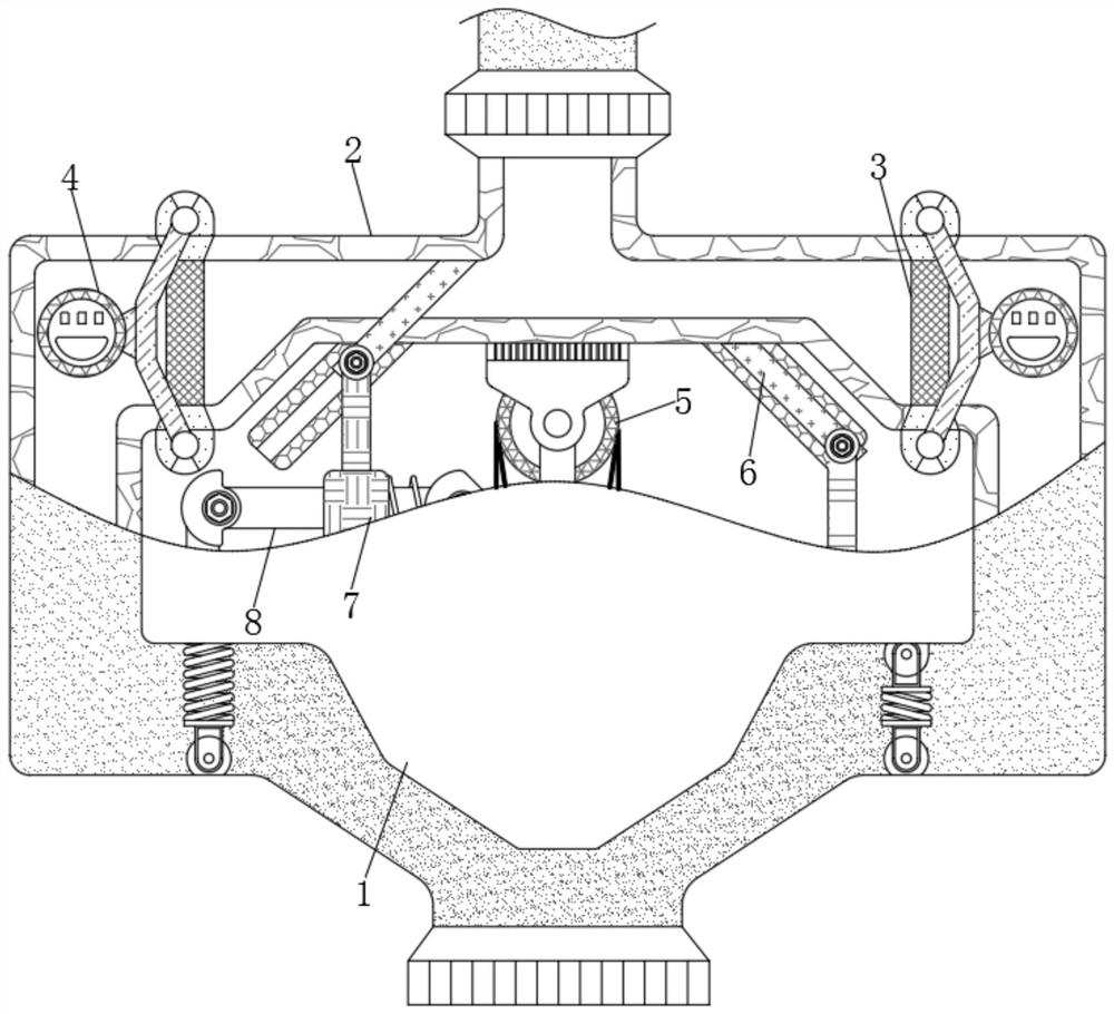
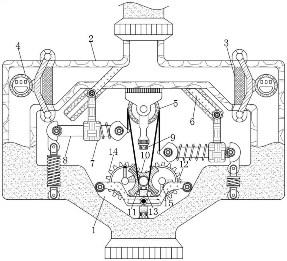
[0022] see Figure 1-3 , a semiconductor wastewater defluorination treatment device, including a shell 1, a treatment chamber 2 is arranged on the outside of the shell 1, and the treatment chamber 2 is composed of a water inlet pipe, a water outlet pipe and a shunt pipe. There are two shunt pipes with the same specification, and the two shunt pipes With the central axis of the outlet pipe as a reference, it presents a symmetrical distribution, and an activated...


PUM


Abstract

The invention relates to the field of semiconductor technology, and discloses a semiconductor wastewater defluorination treatment device, which includes a casing, and a treatment chamber is arranged on the outside of the casing; the gears rotate, and the rotating components rotate synchronously, so that the rotating plate performs intermittent reciprocating rotation, causing the frame to be stuck Intermittently move up and down, the lower plug is far away from the lower socket, the upper plug is snapped into the upper socket, and two heaters are controlled to operate in a staggered manner, which is conducive to the repeated use of the activated alumina layer. The heater operates to dry the activated alumina layer treatment, so that the activated alumina layer can be recycled, avoiding the influence of its subsequent adsorption effect due to excessive adsorption capacity, and effectively improving the effect of wastewater defluorination treatment. The two flow limiting rods are staggered to squeeze the shunt pipe in the treatment chamber to automatically control the flow direction of the waste water, so that it can carry out the defluorination treatment operation without interruption, thereby improving the efficiency of waste water treatment.

Description

technical field [0001] The invention relates to the technical field of semiconductors, in particular to a semiconductor wastewater defluorination treatment device. Background technique [0002] The semiconductor industry is an industry that is very dependent on water resources, and it is also an industry with high water consumption. Therefore, water conservation and waste water recycling have become important measures for semiconductor companies to deal with the water shortage crisis, especially waste water recycling, which can not only reduce the demand for water resources, but also reduce production costs and reduce environmental pollution. Because semiconductor wastewater contains fluorine, if you drink water that does not meet the required fluorine content for a long time, it will cause great harm to human health. At present, when defluorinating wastewater, it is necessary to treat the defluorinating mechanism at regular intervals to avoid long-term use of the defluorin...

Claims


Application Information

Patent Timeline
Patent Type & Authority Patents(China)
IPC IPC(8): C02F1/28C02F101/14
CPCC02F1/281C02F2101/14C02F2303/16
Inventor 周亮夏观强谭珞萍周伟利周源
Owner 深圳市粤昆仑环保实业有限公司
Why Eureka
Try Eureka