interlayer coupler

A coupler and cladding technology, applied in the field of three-dimensional photonics integration, can solve the problems of increasing the overall size of the chip, long coupling length, low error tolerance, etc., and achieve the effects of cost saving, high coupling efficiency, and reduced size

Active Publication Date: 2021-11-26
INST OF SEMICONDUCTORS - CHINESE ACAD OF SCI
View PDF0 Cites 0 Cited by
  • Summary
  • Abstract
  • Description
  • Claims
  • Application Information

AI Technical Summary

Problems solved by technology

The traditional interlayer tapered coupler requires a long coupling length, which greatly increases the overall size of the chip; the vertical directional coupler has high requirements on the size of the structure and processing technology, and has low error tolerance.

Method used


Image

  • interlayer coupler
  • interlayer coupler
  • interlayer coupler

Examples


Embodiment 1

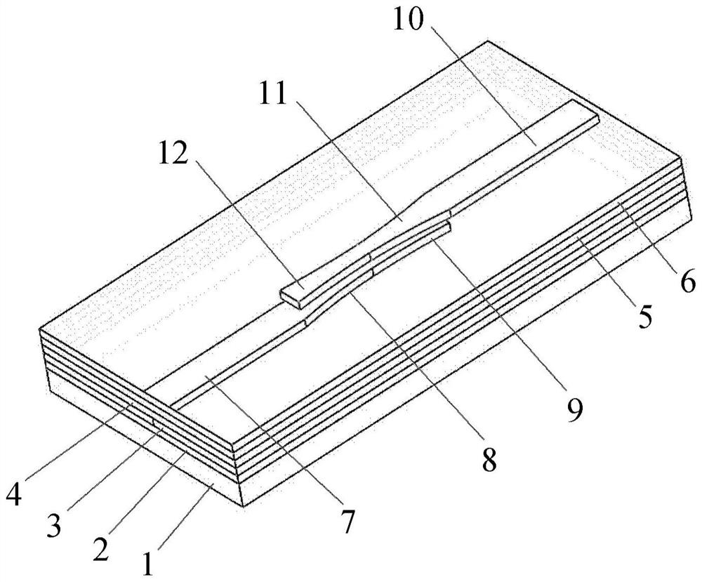
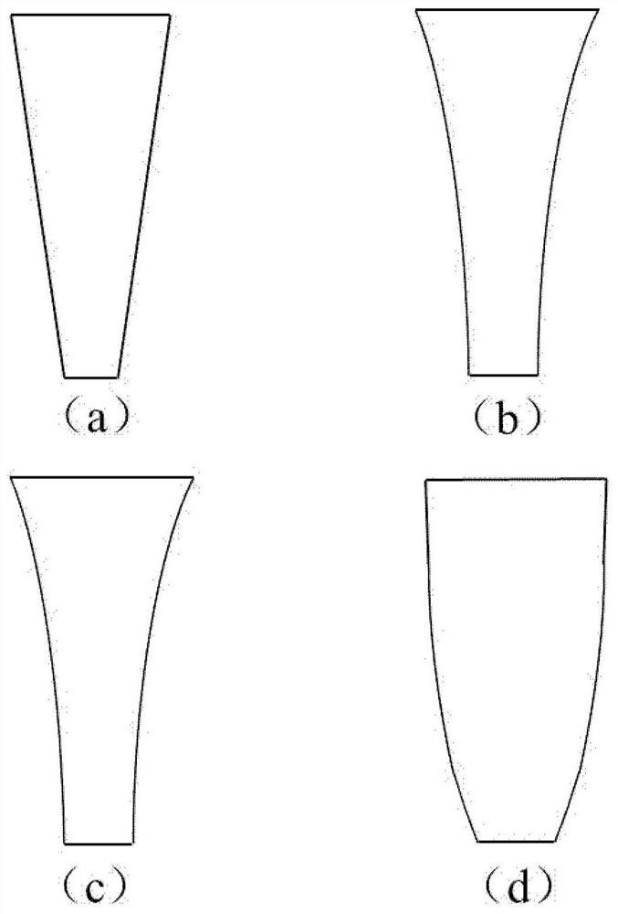
[0081] In this embodiment, using as figure 1 The interlayer coupler structure shown. Wherein, the material of the substrate 1 is silicon, and the thickness is 100 μm. The material of the lower cladding layer 2 and the upper cladding layer 6 is silicon dioxide with a thickness of 2 μm. The material of the middle cladding layer 4 is silicon dioxide with a thickness of 300nm. The material of the first waveguide layer 3 and the second waveguide layer 5 is silicon, and adopts a ridge waveguide structure. The width of each waveguide is 0.5 μm, the thickness is 220 nm, and the thickness of the plate is 70 nm. In the first waveguide layer 3, the widths of each section of waveguide are respectively: the width of the first waveguide 7 is 0.5 μm; in the first tapered waveguide 8, w 1 = 0.2 μm, w 2 =0.5μm, f(z)=z^2; in the second tapered waveguide 9, w 1 = 0.2 μm, w 2 =0.36 μm, f(z)=z^3. In the second waveguide layer 5, the widths of each section of waveguide are respectively: the ...

Embodiment 2

[0087] The difference between this embodiment and Embodiment 1 is that in this embodiment, the first waveguide layer 3 and the second waveguide layer 5 adopt a rectangular waveguide structure, the width of the waveguide is 0.4 μm, and the thickness is 220 nm. In the first waveguide layer 3, the widths of each section of waveguide are respectively: the width of the first waveguide 7 is 0.4 μm; in the first tapered waveguide 8, w i = 0.24 μm, w 2 =0.4μm, f(z)=z^2; in the second tapered waveguide 9, w i = 0.24 μm, w 2 =0.32 μm, f(z)=z^3. In the second waveguide layer 5, the widths of each section of waveguide are respectively: the width of the second waveguide 10 is 0.4 μm; in the third tapered waveguide 11, w 1 = 0.24 μm, w 2 =0.4μm, f(z)=z^2; in the fourth tapered waveguide 12, w i = 0.24 μm, w 2 =0.32 μm, f(z)=z^3. In this embodiment, the above-mentioned four sections of tapered waveguides all have a length of 5 μm, and the formed interlayer coupling region has a length...


PUM

PropertyMeasurementUnit
thicknessaaaaaaaaaa
thicknessaaaaaaaaaa
thicknessaaaaaaaaaa

Abstract

The present disclosure proposes an interlayer coupler, including: a first waveguide layer, a middle cladding layer and a second waveguide layer. Wherein, the first waveguide layer is composed of the first waveguide, the first tapered waveguide and the second tapered waveguide connected sequentially; the width of the first tapered waveguide gradually narrows, and the width of the second tapered waveguide gradually widens; the second tapered waveguide The waveguide layer is composed of the second waveguide, the third tapered waveguide and the fourth tapered waveguide connected sequentially; the width of the third tapered waveguide gradually narrows, and the width of the fourth tapered waveguide gradually widens; the first tapered waveguide and the The fourth tapered waveguide, the second tapered waveguide, and the third tapered waveguide are respectively center-symmetrically distributed, and the spaces of the first tapered waveguide and the second tapered waveguide overlap with the third tapered waveguide and the fourth tapered waveguide Partially forms an interlayer coupling region. The interlayer coupler can shorten the coupling length while ensuring high coupling efficiency, and has a certain tolerance for process deviation.

Description

technical field [0001] The present disclosure relates to the field of three-dimensional photon integration, and in particular to an interlayer coupler. Background technique [0002] As Moore's Law is getting closer and closer to the physical limit, optoelectronic integration solutions with advantages such as high bandwidth, low loss, and small size have become an important way for future development. At present, lasers, modulators, photodetectors, and various passive photonic devices can be compactly integrated on the same substrate, but the two-dimensional integration of each device on the same plane limits the flexibility and integration of the overall chip , so three-dimensional photonic integrated circuit came into being. [0003] The interlayer coupler can realize the three-dimensional free transmission of light between different planes, and provides the possibility to realize the optical interconnection between various devices on different planes. It is a key factor ...

Claims


Application Information

Patent Timeline
Patent Type & Authority Patents(China)
IPC IPC(8): G02B6/26G02B6/122G02B6/12
CPCG02B6/12002G02B6/122G02B6/26
Inventor 李绍洋王玥王亮亮吴远大安俊明
Owner INST OF SEMICONDUCTORS - CHINESE ACAD OF SCI
Why Eureka
Try Eureka