Micro led and its manufacturing method

A technology of miniature and epitaxial wafers, applied in semiconductor/solid-state device manufacturing, semiconductor devices, electrical components, etc., can solve the problems of high cost and large alignment tolerance, achieve uniform spacing, reduce tolerances, and save production costs.

Active Publication Date: 2021-11-23
CHONGQING KONKA PHOTOELECTRIC TECH RES INST CO LTD
View PDF5 Cites 0 Cited by
  • Summary
  • Abstract
  • Description
  • Claims
  • Application Information

AI Technical Summary

Problems solved by technology

The preparation of traditional Micro light emitting diode (Micro light emitting diode, Micro LED) requires four yellow lights, resulting in large alignment tolerances and high costs. How to manufacture high-reliability micro light emitting diodes at low cost is an urgent need to solve question

Method used


Image

  • Micro led and its manufacturing method
  • Micro led and its manufacturing method
  • Micro led and its manufacturing method

Examples


Embodiment Construction

[0026] In order to enable those skilled in the art to better understand the solutions of the present invention, the following will clearly and completely describe the technical solutions in the embodiments of the present invention in conjunction with the drawings in the embodiments of the present invention. Obviously, the described embodiments are only It is an embodiment of a part of the present invention, but not all embodiments. Based on the embodiments of the present invention, all other embodiments obtained by persons of ordinary skill in the art without making creative efforts shall fall within the protection scope of the present invention.

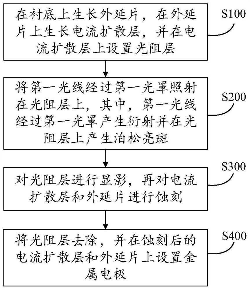
[0027] Before discussing the exemplary embodiments in more detail, it should be mentioned that some exemplary embodiments are described as processes or methods depicted as flowcharts. Although the flowcharts describe the steps as sequential processing, many of the steps may be performed in parallel, concurrently, or simultaneously. ...


PUM


Abstract

The present application relates to a manufacturing method of micro LEDs. The method includes the following operations. An epitaxial wafer is grown on the substrate, a current diffusion layer is grown on the epitaxial wafer, and a photoresist layer is arranged on the current diffusion layer. The first light is irradiated on the photoresist layer through the first mask, and the first light generates Poisson bright spots on the photoresist layer. Develop the photoresist layer, and then etch the current diffusion layer and the epitaxial wafer. The photoresist layer is removed, and metal electrodes are arranged on the etched current diffusion layer and the epitaxial wafer. According to the micro-LED manufacturing method of the application, by using Poisson bright spots for photolithography to prepare cylindrical micro-LEDs, the number of yellow lights can be reduced, production costs can be saved, and the precision and yield of micro-LEDs can be improved.

Description

technical field [0001] The invention relates to the technical field of LED preparation, in particular to a micro LED and a manufacturing method thereof. Background technique [0002] Light-emitting diodes have the advantages of energy saving, environmental protection, and long service life. In the future, light-emitting diodes will gradually replace traditional lighting fixtures such as incandescent lamps and fluorescent lamps, and enter thousands of households. At present, micro light-emitting diodes are a new type of display technology, which has the advantages of high brightness, low delay, long life, wide viewing angle, high contrast, etc., and is the future development direction of light-emitting diodes. The preparation of traditional Micro light emitting diode (Micro light emitting diode, Micro LED) requires four yellow lights, resulting in large alignment tolerances and high costs. How to manufacture high-reliability micro light emitting diodes at low cost is an urgen...

Claims


Application Information

Patent Timeline
Patent Type & Authority Patents(China)
IPC IPC(8): H01L21/027H01L33/00H01L33/14H01L33/36
CPCH01L21/0274H01L33/005H01L33/14H01L33/36H01L2933/0016
Inventor 王涛
Owner CHONGQING KONKA PHOTOELECTRIC TECH RES INST CO LTD
Why Eureka
Try Eureka