

A stable crystal-bonding method for diodes
A diode and stable technology, which is applied in the field of stable die bonding of diodes, can solve the problems that the solder paste is easy to overflow around and affect the reliability of the internal structure of the diode, and achieve a coherent and reliable processing process, stable and reliable internal structure, and stable and reliable shape. Effect
- Summary
- Abstract
- Description
- Claims
- Application Information
AI Technical Summary
Problems solved by technology
Method used
Image

Examples
Embodiment Construction
[0032] In order to further understand the features, technical means, and specific objectives and functions achieved by the present invention, the present invention will be further described in detail below in conjunction with the accompanying drawings and specific embodiments.
[0033] refer to Figure 1 to Figure 6 .
[0034] The embodiment of the present invention discloses a stable crystal bonding method for a diode, which includes the following steps in sequence:
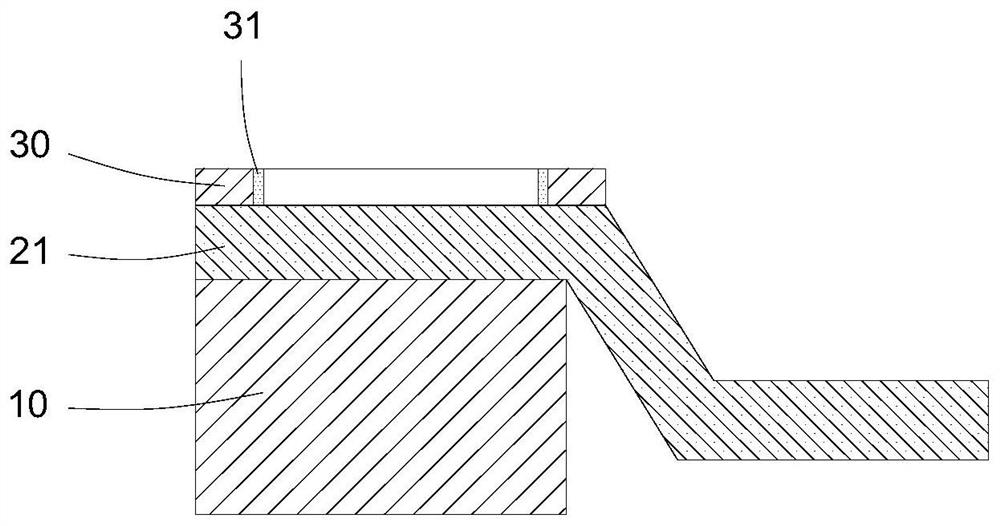
[0035] S1. Preheating the first jig 10, heating the first jig 10, installing the first pin 21 on the first jig 10, can effectively save processing time, and can speed up the plasticity after the subsequent dispensing operation Forming speed of conductive materials;
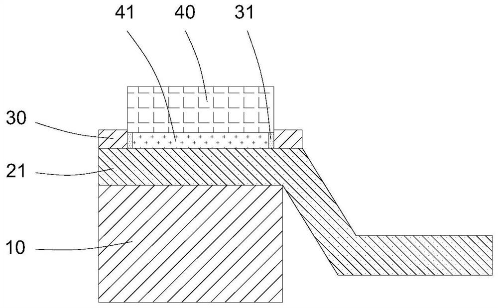
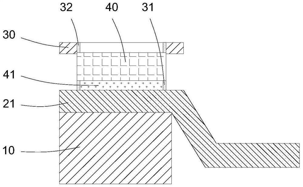
[0036] S2, limit compression, compress the rectangular insulating limit ring 30 on the upper surface of the first pin 21, the top surface area of the first pin 21 is greater than the maximum area of the insulating limit ring 30, that is, the o...
PUM
 Abstract
Description
Claims
Application Information