Packaging method of semiconductor device and semiconductor device

A packaging method and semiconductor technology, applied in semiconductor devices, semiconductor/solid-state device components, semiconductor/solid-state device manufacturing, etc., can solve problems such as affecting heat dissipation effect, low heat transfer efficiency, and increased thermal resistance

Active Publication Date: 2021-06-18
度亘激光技术(苏州)有限公司
View PDF5 Cites 2 Cited by
  • Summary
  • Abstract
  • Description
  • Claims
  • Application Information

AI Technical Summary

Problems solved by technology

[0003] The object of the present invention is to provide a semiconductor device packaging method and a semiconductor device, so as to alleviate the existing high-power semiconductor device packaging process that will form a large number of c

Method used


Image

  • Packaging method of semiconductor device and semiconductor device
  • Packaging method of semiconductor device and semiconductor device
  • Packaging method of semiconductor device and semiconductor device

Examples


Embodiment Construction

[0036] The technical solutions of the present invention will be clearly and completely described below in conjunction with the embodiments. Obviously, the described embodiments are part of the embodiments of the present invention, but not all of them. Based on the embodiments of the present invention, all other embodiments obtained by persons of ordinary skill in the art without making creative efforts belong to the protection scope of the present invention.

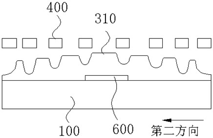
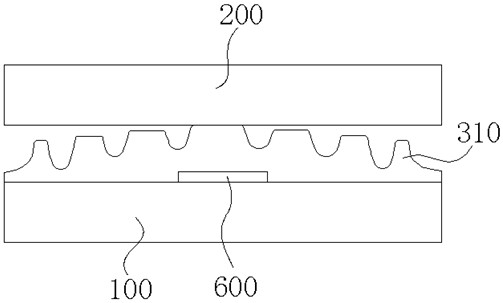
[0037] Such as Figure 1 to Figure 8 As shown, the semiconductor device packaging method provided in this embodiment specifically includes the following steps:

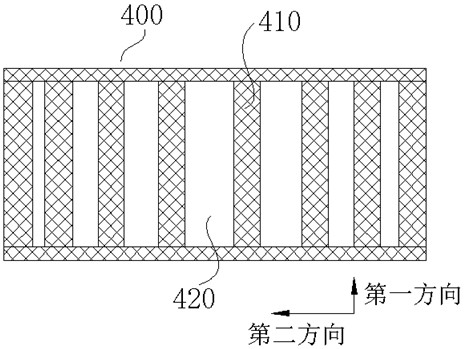
[0038] A mask plate 400 is provided, and the mask plate 400 is provided with a plurality of first openings 420 extending along the first direction and arranged at intervals along the second direction. In the second direction, from the middle of the mask plate 400 to both sides, The widths of the plurality of first openings 420 gradually decrease.

[0039] Util...


PUM


Abstract

The invention provides a packaging method of a semiconductor device and a semiconductor device, and relates to the technical field of semiconductor device packaging. A mask plate with a plurality of first holes is used for evaporating solder on a to-be-welded surface of a first structure, therefore, a plurality of solder protrusions with the heights gradually reduced from the middle of the first structure to the two sides of the first structure are formed on the surface of the solder; in the welding process, the high solder protrusions located in the middle contact with a second structure and are subjected to fusion welding, the low solder protrusions contact with the second structure and achieve welding, and sequential welding is achieved in the direction from the middle to the two sides; gas generated in the welding process and air between the first structure and the second structure can be exhausted from the gaps (a solder groove structures) between two adjacent solder protrusions or the second structure and the top areas of the solder protrusions with the smaller height, so that the probability that holes appear in a solder layer after welding is reduced, the thermal resistance of an interface is reduced, and the heat dissipation effect is improved.

Description

technical field [0001] The invention relates to the technical field of semiconductor device packaging, in particular to a semiconductor device packaging method and the semiconductor device. Background technique [0002] At present, in the packaging process of semiconductor devices, two structural parts are usually welded together by heating the solder. Usually, due to the influence of the viscosity, humidity, wettability and other material properties of the solder and the soldering process method, it will cause A large number of bubbles are generated in the solder layer (on the one hand, the bubbles are formed when the air cannot be discharged during soldering, and on the other hand, the solder flux generates gas when heated), forming voids. For high-power semiconductor devices, when the void rate is large When the temperature is high, it will lead to uneven heat conduction, seriously affect the heat dissipation effect, lead to low heat transfer efficiency, increase thermal ...

Claims


Application Information

Patent Timeline
IPC IPC(8): H01L21/56H01L23/31H01L23/488
CPCH01L21/561H01L23/3121H01L23/488
Inventor 惠利省李靖赵卫东
Owner 度亘激光技术(苏州)有限公司
Why Eureka
Try Eureka