Electronic device shell and manufacturing method thereof

A technology of electronic devices and manufacturing methods, which is applied in the directions of antenna supports/mounting devices, electrical equipment shells/cabinets/drawers, electrical components, etc., which can solve the difficulties of large-scale promotion of LDS technology, difficulty in controlling the consistency of surface metallization, Problems such as the high cost of special modified materials, to achieve the effect of ensuring reliability and appearance, reducing production costs, and improving adhesion

Pending Publication Date: 2021-06-18
昆山哈勃电波电子科技有限公司
View PDF0 Cites 0 Cited by
  • Summary
  • Abstract
  • Description
  • Claims
  • Application Information

AI Technical Summary

Problems solved by technology

Therefore, in the prior art, the LDS process is used to form the antenna wiring on the housing of the electronic device, but the cost of special modified materials suitable for LDS is relatively high, and the parameters of different modified materials are different. , the consistency of surface metallization treatment is difficult to control, which makes it difficult to promote the LDS process on a large scale

Method used


Image

  • Electronic device shell and manufacturing method thereof
  • Electronic device shell and manufacturing method thereof
  • Electronic device shell and manufacturing method thereof

Examples


Embodiment Construction

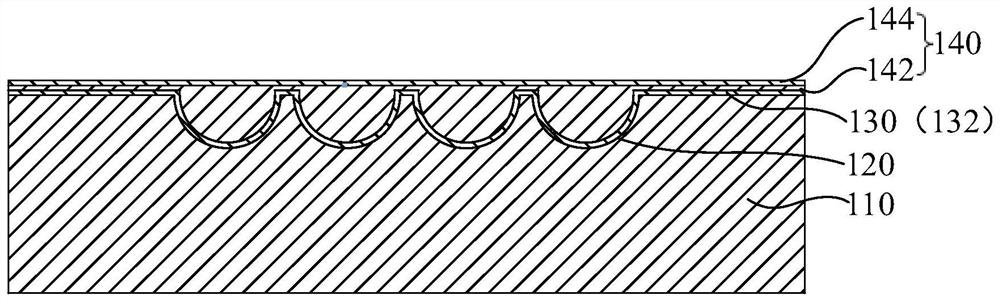
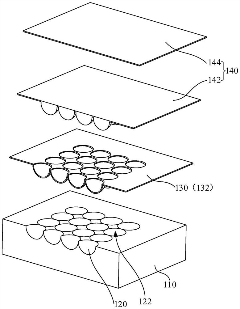
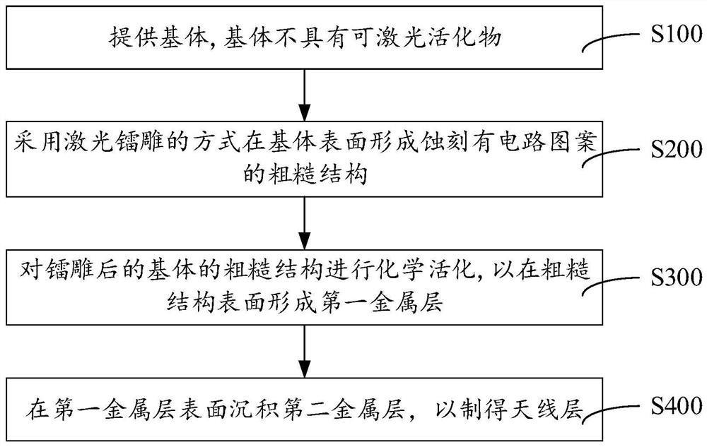
[0024] In order to facilitate the understanding of the present invention, the present invention will be described more fully below with reference to the associated drawings. Preferred embodiments of the invention are shown in the accompanying drawings. However, the present invention can be embodied in many different forms and is not limited to the embodiments described herein. On the contrary, these embodiments are provided to make the understanding of the disclosure of the present invention more thorough and comprehensive.

[0025] It should be noted that when an element is referred to as being “fixed” to another element, it can be directly on the other element or there can also be an intervening element. When an element is referred to as being "connected to" another element, it can be directly connected to the other element or intervening elements may also be present.

[0026] Unless otherwise defined, all technical and scientific terms used herein have the same meaning as...


PUM


Abstract

The invention relates to an electronic device shell and a manufacturing method thereof. The electronic device shell comprises a base body, a first metal layer and a second metal layer, the base body is not provided with a laser activator, and a rough structure etched with a circuit pattern is formed on the surface of the base body in a laser etching mode; the first metal layer is formed on the surface of the rough structure; and the second metal layer is an antenna layer and is formed on the surface of the first metal layer. The base body used by the electronic device shell is not limited by an LDS process and laser etching equipment, the selection range of the types of the base body and the laser etching equipment is widened, the reliability and the appearance performance of a product are guaranteed, and the production cost of the electronic device shell is reduced. In addition, the rough structure is formed on the surface of the base body in the laser etching manner so that the adhesive force of the antenna layer relative to the base body can be improved.

Description

technical field [0001] The invention relates to the technical field of laser forming technology, in particular to an electronic device casing and a manufacturing method thereof. Background technique [0002] LDS refers to the technology of using a computer to control the movement of the laser according to the trajectory of the conductive pattern, projecting the laser onto the molded three-dimensional plastic device, and activating the circuit pattern in a short period of time. However, the material suitable for the LDS process is a special modified material containing laser activatable substances, which can be activated by laser activators to release metal particles after laser irradiation. At present, the LDS process can be used on modified plastics after laser irradiation. Form metallization directly. Therefore, in the prior art, the LDS process is used to form the antenna wiring on the housing of the electronic device, but the cost of special modified materials suitable ...

Claims


Application Information

Patent Timeline
Patent Type & Authority Applications(China)
IPC IPC(8): H05K5/02H01Q1/38H01Q1/22
CPCH01Q1/22H01Q1/38H05K5/0247
Inventor 郁军杨群坤陈二凯
Owner 昆山哈勃电波电子科技有限公司
Why Eureka
Try Eureka