

PCB (Printed Circuit Board) and potential connection side surface metallization process thereof
A PCB board and metallization technology, which is applied in the field of metallization technology on the side of the PCB board and its potential connection, can solve the problems affecting the normal operation of the circuit board, the separation of the copper layer from the circuit board, etc., and achieve a simple manufacturing method and high production efficiency. Effect
- Summary
- Abstract
- Description
- Claims
- Application Information
AI Technical Summary
Problems solved by technology
Method used
Image

Examples
Embodiment Construction
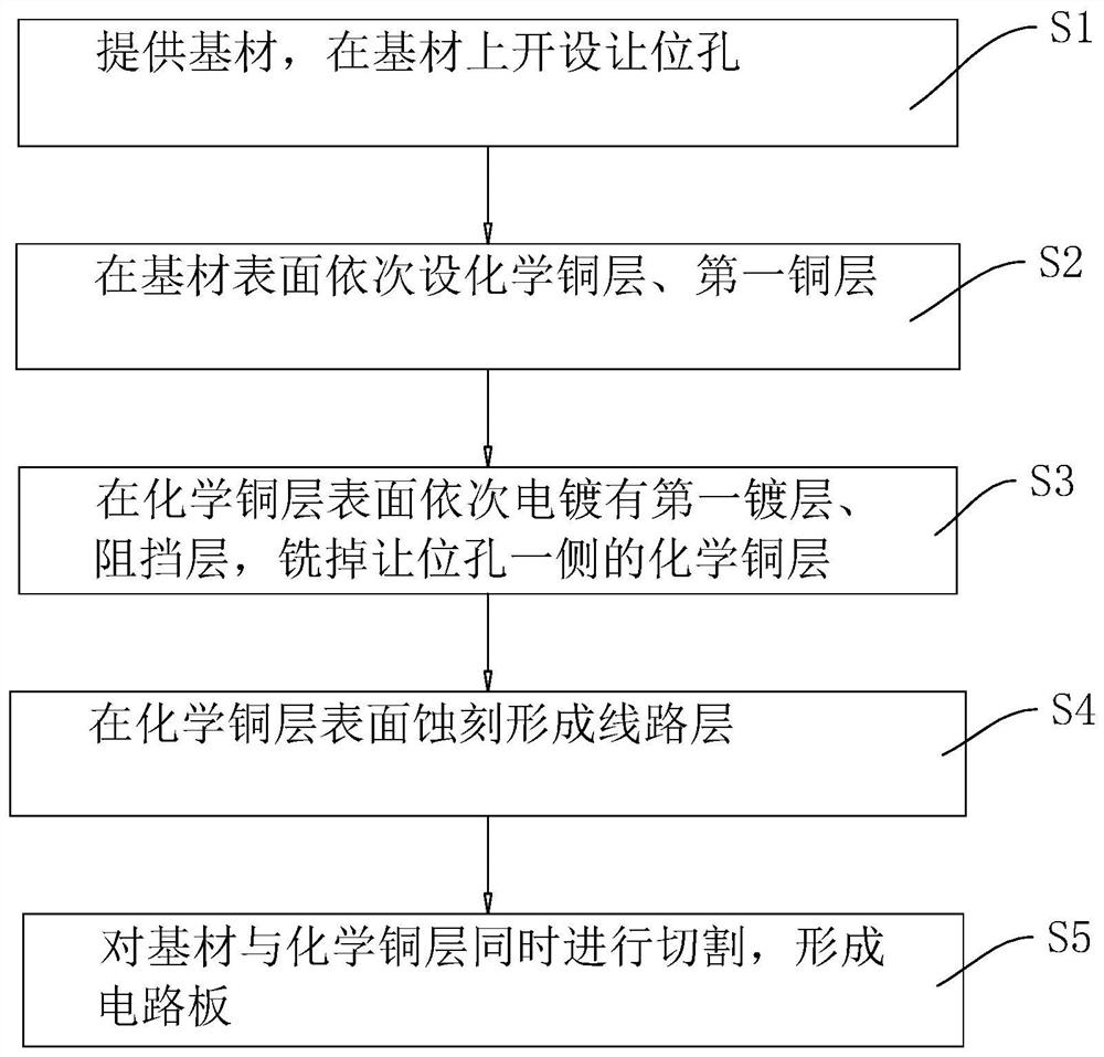
[0038] The following is attached Figure 1-5 The application is described in further detail.
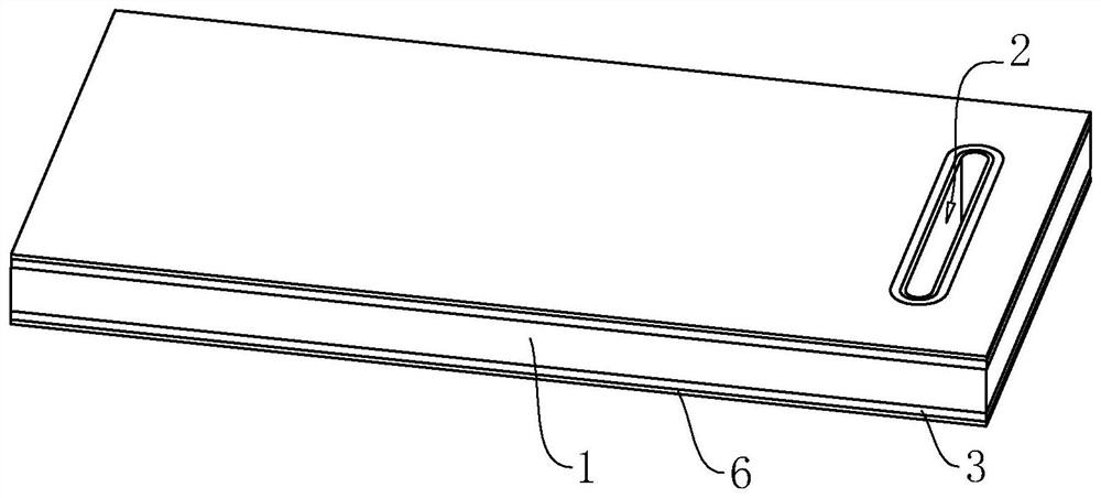
[0039] The first aspect: the embodiment of the present application discloses a PCB board.
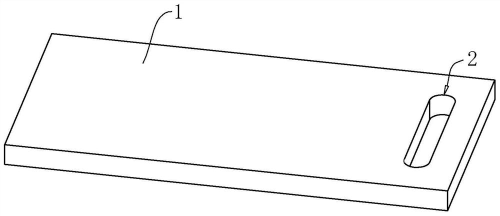
[0040] refer to Figure 5 , a PCB board includes a substrate 1, a substrate 1, two circuit layers 11 respectively arranged on opposite sides of the substrate 1, and a connector connected to the two circuit layers 11. In this embodiment, the connection The component is the first plating layer 5 formed by copper plating, the opposite ends of the first plating layer 5 are respectively connected to the two circuit layers 11, and the first plating layer 5 is attached to the side wall of the substrate 1 close to the socket.
[0041] In the second aspect, the embodiment of the present application discloses a metallization process for the potential side of a PCB board.
[0042] A metallization process on the side of the PCB board connected to the potential, refer to figure 1 , which includes the f...
PUM
 Abstract
Description
Claims
Application Information