Vertical integrated unit light emitting diode

A technology of light-emitting diodes and integrated units, applied in electrical components, nanotechnology, electro-solid devices, etc., can solve the problems of LED light efficiency, heat dissipation and stability limitations, etc., to improve light extraction efficiency, optimize heat dissipation performance, and solve luminous Effects of uneven problems

Active Publication Date: 2021-06-25
纳微朗科技(深圳)有限公司
View PDF7 Cites 0 Cited by
  • Summary
  • Abstract
  • Description
  • Claims
  • Application Information

AI Technical Summary

Problems solved by technology

Therefore, LED light efficiency, heat dissipation and stability under high current will be severely limited

Method used


Image

  • Vertical integrated unit light emitting diode
  • Vertical integrated unit light emitting diode
  • Vertical integrated unit light emitting diode

Examples


Embodiment 1

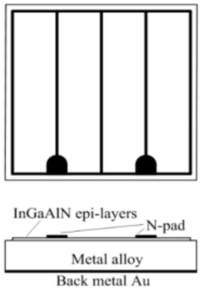
[0060] This embodiment provides a vertically integrated unit light-emitting diode, including: a second conductivity type electrode 1, an overall mesa structure 6 composed of a diode unit mesa structure, a groove 7 and a diode unit 8, a second conductivity type electrode line 9, and a pad 10. The second conductivity type electrode 1 is an N-type conductivity electrode. The width of the groove is 0.1 micron, and the depth is 0.01 micron. The groove is located between the diode units, and a linear electrode line is laid in the groove. The width of the electrode line is 0.01 micron to 10 micron, and the thickness is 0.01 micron to 10 micron. The N-type conductive electrode is in ohmic contact with the top of the diode unit and is connected to the pad through a strip-shaped electrode line. The number of pads is 1, and the shape is an irregular polygon with an arc-shaped side, located on the short edge of the mesa structure. The pad thickness is 0.1 micron and the width is 50 micro...

Embodiment 2

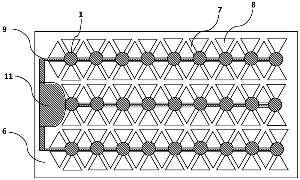
[0068] This embodiment provides a vertically integrated unit light emitting diode, such as Figure 8 As shown, it includes: a second conductivity type electrode 1, an overall mesa structure 6, a trench 7, a diode unit 8, a second conductive type electrode line 9 and a pad 10, and the second conductive type electrode 1 is an N-type conductive electrode. The width of the groove is 1 micron, and the depth is 0.1 micron. The groove structure is located between the diode units, and a linear electrode line is laid in the groove. The width of the electrode line is 0.1 micron to 1 micron, and the thickness is 0.1 micron to 1 micron. The N-type conductive electrode is in ohmic contact with the top of the diode unit and is connected to the pad through a strip-shaped electrode line. The number of pads is 1, the shape is a rectangle with rounded corners, it is located in the middle of the table, the thickness of the pad is 1 micron, and the width is 5 microns.

[0069] The chip includes ...


PUM

PropertyMeasurementUnit
lengthaaaaaaaaaa
thicknessaaaaaaaaaa
widthaaaaaaaaaa

Abstract

The invention provides a vertical integrated unit light emitting diode, which comprises n diode mesa structures and groove structures formed on one side far away from a first conductive type electrode, wherein a second conductive type electrode wire extends along grooves on a second conductive type layer, the distance between adjacent diode units in the direction perpendicular to the extension direction of the second conductive type electrode wire is determined according to a current diffusion length, n diode units comprise current blocking layers and protective metal layers, reflectors are arranged in the protective metal layers, and the current blocking layers are embedded in the protective metal layers and the reflectors. According to the invention, diffusion of current in the vertical direction is effectively blocked, and the transverse diffusion of the current is promoted through geometric optimization with high degree of freedom and small enough micro-nano structure design of the unit diode, so that the problem of uneven light emitting caused by uneven current diffusion is solved, and photoelectric conversion efficiency / lumen efficiency is improved.

Description

technical field [0001] The invention relates to the field of semiconductor materials and device technology, especially semiconductor optoelectronic devices, and more specifically, the invention relates to a vertically integrated unit light emitting diode. Background technique [0002] In conventional vertical structure LED chips, the current diffusion mainly depends on the N-type conductive electrode side, and there are electrode lead-type leads or drill-type leads, but the overall current diffusion is still uneven, resulting in loss of luminous efficiency and uneven heat dissipation, thus Affects the efficiency and stability of the unit diode chip. This restricts vertical high-power LED chips from providing products with higher lumen output per unit area. Uneven current diffusion, uneven thermal diffusion, and uneven light extraction lead to great limitations in the three important parameters of lumen efficiency, lumen density output, and lumen cost. The vertical LED chip ...

Claims


Application Information

Patent Timeline
Patent Type & Authority Applications(China)
IPC IPC(8): H01L33/38H01L33/14H01L33/20H01L33/64H01L33/10H01L27/15B82Y40/00
CPCH01L33/145H01L33/38H01L33/20H01L33/10H01L33/642H01L33/385H01L27/156B82Y40/00
Inventor 闫春辉蒋振宇
Owner 纳微朗科技(深圳)有限公司
Why Eureka
Try Eureka