
Wlcsp package with different solder volumes

A technology of solder and contact pad, applied in the direction of electric solid-state devices, semiconductor devices, semiconductor/solid-state device components, etc., can solve the problems of increasing WLCSP board-level reliability, increasing demand, increasing resistance, etc.

Pending Publication Date: 2021-06-29
STMICROELECTRONICS SRL
View PDF0 Cites 0 Cited by
  • Summary
  • Abstract
  • Description
  • Claims
  • Application Information

AI Technical Summary

Problems solved by technology

[0003] As the need to provide more WLCSPs in electronic devices to perform functions of increasing complexity increases, while at the same time reducing manufacturing costs, increasing resistance to external stress to reduce the possibility of failure, and increasing Board-level reliability of WLCSP, there are significant challenges in balancing all the above preferences

Method used


Image

  • Wlcsp package with different solder volumes
  • Wlcsp package with different solder volumes
  • Wlcsp package with different solder volumes

Examples


Embodiment Construction

[0020] In the following description, numerous specific details are set forth in order to provide a thorough understanding of various embodiments of the present disclosure. However, one skilled in the art will understand that the present disclosure may be practiced without these specific details. In other instances, well-known structures associated with electronic components and semiconductor fabrication techniques have not been described in detail to avoid unnecessarily obscuring the description of embodiments of the present disclosure.

[0021] Unless the context otherwise requires, throughout the following specification and claims, the word "comprising" and variations thereof (such as including and "comprising") are to be interpreted in an open inclusive sense, ie, interpreted as "comprising" but not limited to".

[0022] The use of ordinal numbers such as first, second, and third does not necessarily imply the meaning of an ordered order, but may merely distinguish multipl...


PUM


Abstract

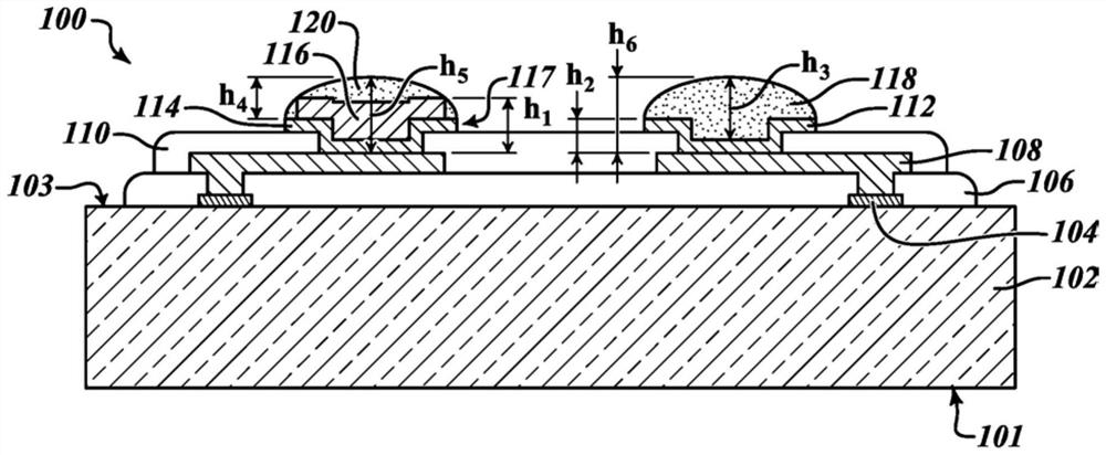
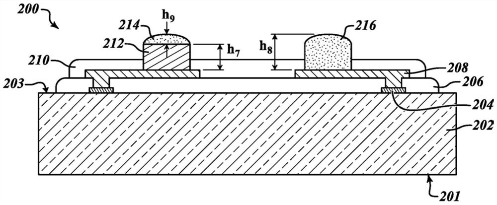
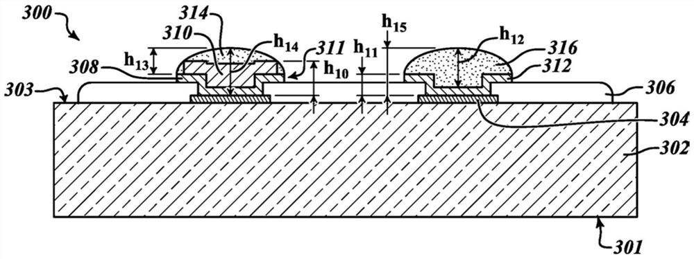
The embodiment of the invention relates to a WLCSP package with different solder volumes. The present disclosure is directed to a wafer level chip scale package (WLCSP) with various combinations of contacts and Under Bump Metallizations (UBMs) having different structures and different amounts solder coupled to the contacts and UBMs. Although the contacts have different structures and the volume of solder differs, the total standoff height along the WLCSP remains substantially the same. Each portion of solder coupled to each respective contact and UBM includes a point furthest away from an active surface of a die of the WLCSP. Each point of each respective portion of solder is co-planar with each other respective point of the other respective portions of solder. Additionally, the contacts with various and different structures are positioned accordingly on the active surface of the die of the WLCSP to reduce failures that may result from the WLCSP being exposed to thermal cycling or the WLCSP being dropped.

Description

technical field [0001] The present disclosure relates to a wafer level chip scale package (WLCSP) including contacts and solder bumps. Background technique [0002] Typically, a semiconductor device package, such as a chip scale package or wafer level chip scale package (WLCSP), is electrically coupled to a printed circuit board (PCB) by solder bumps or conductive adhesive material having the same shape, height and volume . [0003] As the need to provide more WLCSPs in electronic devices to perform functions of increasing complexity increases while reducing manufacturing costs, increasing resistance to external stress to reduce the likelihood of failure, and increasing Board-level reliability for WLCSP, balancing all of the above preferences presents significant challenges. Examples of electronic devices include notebook computers, monitors, televisions, smart phones, tablet computers, or any other electronic device. SUMMARY OF THE INVENTION [0004] Embodiments of the...

Claims


Application Information

Patent Timeline
Patent Type & Authority Applications(China)
IPC IPC(8): H01L23/488
CPCH01L24/14H01L2224/1403H01L2924/3512H01L2924/35121H01L2224/131H01L24/06H01L24/13H01L2224/0401H01L24/02H01L2224/05558H01L2224/0603H01L2224/0601H01L2224/1401H01L2224/14051H01L2224/14505H01L2224/02377H01L2224/0236H01L24/11H01L2224/1147H01L2224/1132H01L2224/133H01L2224/13294H01L2224/0239H01L2224/05569H01L2224/05559H01L2224/05557H01L2224/0346H01L2224/03452H01L2224/0345H01L2224/0231H01L2224/05024H01L2224/05018H01L2224/05019H01L2224/05017H01L2224/05647H01L2224/05644H01L2224/05639H01L2224/05564H01L2224/0347H01L2224/13144H01L2224/13147H01L2224/13139H01L2224/11849H01L2224/13026H01L2224/13007H01L2224/14179H01L24/05H01L24/03H01L2224/05008H01L2224/0348H01L2224/119H01L2224/06102H01L2224/05147H01L2224/05073H01L2224/13006H01L2224/13562H01L2224/136H01L2224/138H01L2224/13794H01L2224/13022H01L2224/06051H01L2224/16227H01L24/16H01L2224/06179H01L2224/13076H01L2924/014H01L2924/00012H01L2924/00014H01L2924/01029H01L2924/01047H01L2924/01044H01L2224/03H01L2224/11H01L23/49816H01L2224/13028
Inventor D·加尼
Owner STMICROELECTRONICS SRL
Learn More