Supercharge Your Innovation With Domain-Expert AI Agents!

Array substrate, array substrate manufacturing method and display panel

A technology of array substrates and substrates, applied in the direction of final product manufacturing, sustainable manufacturing/processing, climate sustainability, etc., can solve the problems of weak electric field, affecting the sensitivity of photosensitive sensors, and inability to effectively separate photogenerated electrons and holes.

Active Publication Date: 2022-07-12
WUHAN CHINA STAR OPTOELECTRONICS TECH CO LTD
View PDF0 Cites 0 Cited by
  • Summary
  • Abstract
  • Description
  • Claims
  • Application Information

AI Technical Summary

Problems solved by technology

Since the P-α-Si grown by ion implantation or plasma enhanced chemical vapor deposition (Plasma Enhanced Chemical Vapor Deposition, PECVD) is at the top of the incident light, far away from the junction region of the heterojunction, the electric field is weak and cannot Effective separation of photogenerated electrons and holes, seriously affecting the sensitivity of the photosensitive sensor

Method used


Image

  • Array substrate, array substrate manufacturing method and display panel
  • Array substrate, array substrate manufacturing method and display panel
  • Array substrate, array substrate manufacturing method and display panel

Examples


Embodiment Construction

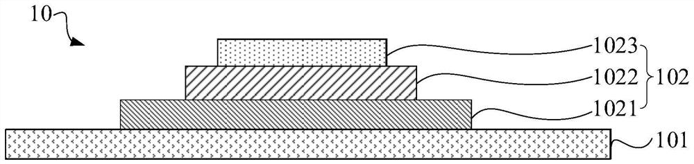
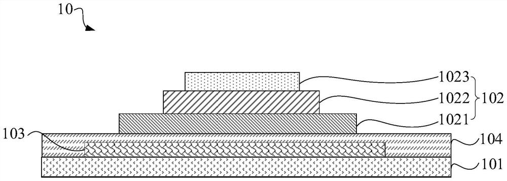
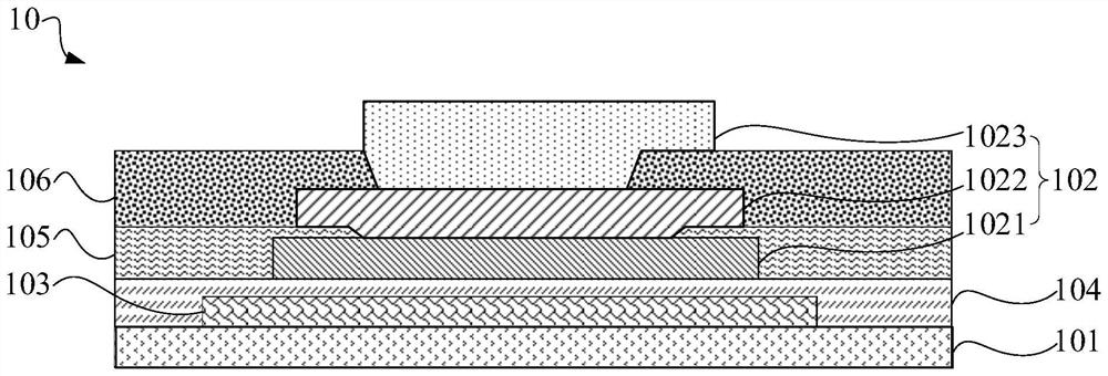
[0039] The technical solutions in the present invention will be clearly and completely described below with reference to the accompanying drawings in the present invention. Obviously, the described embodiments are only some, but not all, embodiments of the present invention. Based on the embodiments of the present invention, all other embodiments obtained by those skilled in the art without creative efforts shall fall within the protection scope of the present invention.

[0040] It should be noted that, in the description of the present invention, it should be understood that the terms "upper", "lower", "front", "rear", "left", "right", "inner", "outer", etc. The indicated orientation or positional relationship is based on the orientation or positional relationship shown in the accompanying drawings, which is only for the convenience of describing the present invention and simplifying the description, rather than indicating or implying that the indicated device or element mus...


PUM

PropertyMeasurementUnit
thicknessaaaaaaaaaa
thicknessaaaaaaaaaa
thicknessaaaaaaaaaa

Abstract

The invention discloses an array substrate, a manufacturing method of the array substrate and a display panel. The array substrate includes a substrate and a photosensitive element. The photosensitive element is arranged on the substrate, and the photosensitive element includes a doped semiconductor layer, an intrinsic semiconductor layer and a transparent electrode layer that are stacked in sequence; wherein, the doped semiconductor layer is an N-type doped semiconductor, so The transparent electrode layer is a P-type transparent electrode, or the doped semiconductor layer is a P-type doped semiconductor, and the transparent electrode layer is an N-type transparent electrode. By improving the internal structure of the photosensitive element, the absorption of light by the incident interface of the intrinsic semiconductor layer can be enhanced, thereby enhancing the sensitivity of the photosensitive element.

Description

technical field [0001] The present invention relates to the field of display technology, and in particular, to an array substrate, a method for manufacturing the array substrate, and a display panel. Background technique [0002] With the rapid development of the panel industry, in addition to the requirements for high resolution, wide viewing angle, and low power consumption of displays, other requirements are also placed on display panels. Enriching panel functions, increasing human-computer interaction, and improving the competitiveness of display panels are one of the main development directions of display panels at present. [0003] Optical fingerprints, ambient light sensors and other photosensitive elements (sensors) are currently developing in a relatively hot direction. At present, the production process of the panel factory often uses polysilicon (poly-Si) to make the light-absorbing layer of the photosensitive sensor, but the thickness of the poly-Si photosensiti...

Claims


Application Information

Patent Timeline
Patent Type & Authority Patents(China)
IPC IPC(8): H01L27/12H01L27/32
CPCH01L27/1222H01L27/1259H01L27/127H10K59/60Y02P70/50H10K59/126H10K59/879G02F1/13312G02F1/1362H10K59/8792G02F1/136209
Inventor 龚帆艾飞宋继越
Owner WUHAN CHINA STAR OPTOELECTRONICS TECH CO LTD
Features
  • R&D
  • Intellectual Property
  • Life Sciences
  • Materials
  • Tech Scout
  • Unparalleled Data Quality
  • Higher Quality Content
  • 60% Fewer Hallucinations
Learn More