Method for forming semiconductor structure

A semiconductor and work function technology, applied in semiconductor/solid-state device manufacturing, electrical components, circuits, etc., can solve problems such as transistor performance needs to be improved, achieve the effects of accurate thickness, simplified process, and improved production efficiency

Pending Publication Date: 2021-07-09
SEMICON MFG INT (SHANGHAI) CORP +1
View PDF0 Cites 0 Cited by
  • Summary
  • Abstract
  • Description
  • Claims
  • Application Information

AI Technical Summary

Problems solved by technology

[0004] However, the performance of existing transistors still needs to be improved

Method used


Image

  • Method for forming semiconductor structure
  • Method for forming semiconductor structure
  • Method for forming semiconductor structure

Examples


Embodiment Construction

[0028] As mentioned in the background art, the performance of existing transistors still needs to be improved. Now analyze and illustrate in conjunction with specific embodiment.

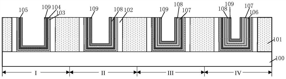
[0029] figure 1 It is a schematic cross-sectional structure diagram of a semiconductor structure in an embodiment.

[0030] Please refer to figure 1 , including: a substrate 100, which includes a first region I, a second region II, a third region III and a fourth region IV; a dielectric layer 101 on the substrate 100; a dielectric layer on the first region I The first gate opening (not shown) in 101, the second gate opening (not shown) in the upper dielectric layer 101 of the second region II, the third gate opening (not shown) in the upper dielectric layer 101 of the third region III electrode opening (not shown), the fourth gate opening (not shown) located in the dielectric layer 101 on the fourth region IV, the sidewall of the first gate opening, the sidewall of the second gate opening, the th...


PUM


Abstract

A method for forming a semiconductor structure comprises the following steps: providing a substrate which comprises a first region, a second region and a third region; forming a first work function material layer on the first region, the second region and the third region of the substrate; forming a second work function material layer on the first work function material layer, wherein the work function types of the second work function material layer and the first work function material layer are the same; removing the first work function material layer and the second work function material layer on the first region; and removing the second work function material layer on the second region. The performance of the formed semiconductor structure is improved.

Description

technical field [0001] The invention relates to the field of semiconductor manufacturing, in particular to a method for forming a semiconductor structure. Background technique [0002] In the field of integrated circuit manufacturing, as the size of transistors continues to shrink, the physical limits of devices have an increasing impact on device fabrication, and it becomes more difficult to scale down the feature size of devices. Among them, transistors and their circuit manufacturing The difficulty of the field has also increased significantly. [0003] In order to meet the requirements, it is necessary to form transistors with different functions on the same substrate. In the prior art, a work function layer is used to adjust the performance of transistors formed by post-metal gate technology to meet the requirements of transistors with different functions. [0004] However, the performance of existing transistors has yet to be improved. Contents of the invention [...

Claims


Application Information

Patent Timeline
IPC IPC(8): H01L21/8234
CPCH01L21/823437H01L21/823456H01L21/823462
Inventor 陈建
Owner SEMICON MFG INT (SHANGHAI) CORP
Why Eureka
Try Eureka