
Patterning method and semiconductor structure

A technique for patterning, structural defects

Active Publication Date: 2021-07-09
CHANGXIN MEMORY TECH INC
View PDF4 Cites 2 Cited by
  • Summary
  • Abstract
  • Description
  • Claims
  • Application Information

AI Technical Summary

Problems solved by technology

[0003] In the double patterning method of the prior art, due to the structural difference between the storage area and the peripheral circuit area, different etching load effects will be generated during the patterning process, resulting in misalignment of critical dimensions after patterning, which in turn causes the storage area Structural defects occur near the peripheral circuit area

Method used


Image

  • Patterning method and semiconductor structure
  • Patterning method and semiconductor structure
  • Patterning method and semiconductor structure

Examples


Embodiment Construction

[0066]Example embodiments will now be described more fully with reference to the accompanying drawings. Example embodiments may, however, be embodied in many forms and should not be construed as limited to the embodiments set forth herein; rather, these embodiments are provided so that this disclosure will be thorough and complete, and will fully convey the concept of example embodiments to those skilled in the art. The same reference numerals in the drawings denote the same or similar structures, and thus their detailed descriptions will be omitted.

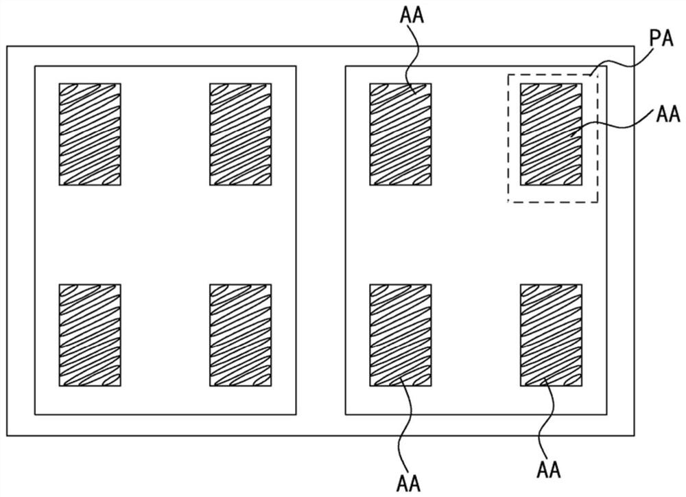
[0067] Such as figure 1 as shown, figure 1 Shown is a top view of a semiconductor structure. figure 1 Two storage units (BANK) are schematically shown in , each storage unit includes a plurality of storage areas AA. The number of storage areas AA provided in each storage unit may be two, four, six, eight, ten, etc. A peripheral circuit area PA is provided adjacent to the periphery of the storage area AA. The storage area A...


PUM


Abstract

Embodiments of the invention provide a patterning method and a semiconductor structure. The method comprises the following steps: providing a substrate which comprises a storage region and a peripheral circuit region which are adjacent to each other; forming a pattern transfer layer with a plurality of first hard masks on the substrate, wherein the first hard masks extend in the first direction and are arranged at intervals; forming a barrier layer on the pattern transfer layer; forming a plurality of second hard masks extending along a second direction on the barrier layer, wherein the second hard masks are arranged at intervals, and the second hard masks are located on the storage area and have structural defects at positions close to the peripheral circuit area; forming a first buffer layer on the barrier layer, and filling the first buffer layer with a second hard mask with structural defects, wherein the orthographic projection of the first buffer layer coincides with the peripheral circuit area and a part of the storage area; and patterning the barrier layer and the pattern transfer layer by taking the first buffer layer and the second hard mask which is not filled with the first buffer layer as masks.

Description

technical field [0001] The present invention relates to the technical field of semiconductors, in particular to a patterning method and a semiconductor structure. Background technique [0002] A dynamic random access memory (DRAM) includes an array area composed of a plurality of memory cells, and a peripheral area where a control circuit is located. With the continuous reduction of the size of semiconductor devices, in order to improve the integration of devices, a double patterning process (self-aligned-doubled patterning, SADP) is proposed. [0003] In the double patterning method of the prior art, due to the structural difference between the storage area and the peripheral circuit area, different etching load effects will be generated during the patterning process, resulting in misalignment of critical dimensions after patterning, which in turn causes the storage area Structural defects are generated at portions close to the peripheral circuit region. Therefore, how to...

Claims


Application Information

Patent Timeline
Patent Type & Authority Applications(China)
IPC IPC(8): H01L21/8242H01L27/108H10B12/00
CPCH10B12/30H10B12/09
Inventor 宛强夏军占康澍李森刘涛徐朋辉
Owner CHANGXIN MEMORY TECH INC
Learn More