A kind of manufacturing method of LED epitaxial wafer

A technology for LED epitaxial wafers and a manufacturing method, which is applied to semiconductor devices, electrical components, circuits, etc., can solve problems such as hindering LED performance, low brightness of LED epitaxial wafers, and reducing energy-saving effects, so as to improve antistatic ability and increase wavelength. Uniformity, the effect of improving wavelength concentration

Active Publication Date: 2022-07-19
XIANGNENG HUALEI OPTOELECTRONICS
View PDF6 Cites 0 Cited by
  • Summary
  • Abstract
  • Description
  • Claims
  • Application Information

AI Technical Summary

Problems solved by technology

[0003] At present, the brightness of the LED epitaxial wafer prepared by the existing LED epitaxial wafer production method is not high, which seriously hinders the improvement of LED performance and reduces the energy-saving effect of LED.
[0004] In summary, there is an urgent need for a method for manufacturing LED epitaxial wafers to solve the problem of low brightness of LED epitaxial wafers in the prior art.

Method used


Image

  • A kind of manufacturing method of LED epitaxial wafer
  • A kind of manufacturing method of LED epitaxial wafer

Examples


Embodiment 1

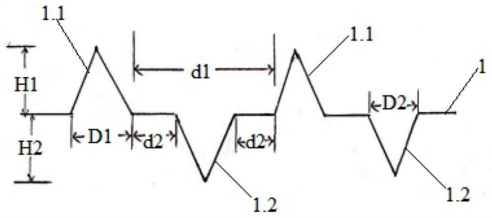
[0033] see figure 1 , a method for making an LED epitaxial wafer, comprising the following steps:

[0034] Step 3, making a plurality of raised cones 1.1 on the AlN layer 1 at intervals;

[0035] Step 4. A plurality of concave and inverted conical cavities 1.2 are formed on the AlN layer 1 at intervals, and the conical cavities 1.2 and the cones 1.1 are staggered and not connected to each other, that is, between any two adjacent conical cavities 1.2 A cone 1.1 is set, and a cone cavity 1.2 is set between any two adjacent cones 1.1;

[0036] Step 5. Periodically grow a plurality of multi-quantum well light-emitting layers on the AlN layer 1, each of which includes an InGaN well layer and a GaN barrier layer grown in sequence, wherein the multi-quantum well light-emitting layers grown in the first period are The well light-emitting layer is used to fill the conical cavity 1.2 in the step 4. Starting from the second cycle, the multi-quantum well light-emitting layers grown in t...

Embodiment 2

[0050] The difference from Example 1 is that in step 3, D1 is 1000 nm, height H1 is 850 nm, and the shortest distance d1 between the bottom surfaces of adjacent cones 1.1 is 2100 nm. In step 4, D2 is 800 nm, and height H2 is 850 nm. The shortest distance d2 between the top surface of the conical cavity 1.2 and the bottom surface of the adjacent cone 1.1 is 500 nm, and the thickness of the AlN layer 1 is 1800 nm.

Embodiment 3

[0052] The difference from Example 1 is that in step 3, D1 is 1100 nm, height H1 is 900 nm, and the distance d1 between the bottom surfaces of adjacent cones 1.1 is 2200 nm. In step 4, D2 is 900 nm, and height H2 is 900 nm. The shortest distance d2 between the top surface of the cavity 1.2 and the bottom surface of the adjacent cone 1.1 is 600 nm, and the thickness of the AlN layer 1 is 2000 nm.


PUM

PropertyMeasurementUnit
thicknessaaaaaaaaaa
thicknessaaaaaaaaaa
thicknessaaaaaaaaaa

Abstract

The present invention provides a method for manufacturing an LED epitaxial wafer, which includes the following steps: step 3: making a plurality of convex cones at intervals on the AlN layer; step 4: making a plurality of concave and inverted cones at intervals on the AlN layer Cavity, the conical cavity and the cone are staggered and not connected to each other; step 5, periodically grow a plurality of multiple quantum well light-emitting layers on the AlN layer, each of the multiple quantum well light-emitting layers includes sequentially grown InGaN The well layer and the GaN barrier layer, wherein the multi-quantum well light-emitting layer grown in the first cycle is used to fill the conical cavity in the step 4, and starting from the second cycle, the multi-quantum well light-emitting layer grown in the subsequent cycle is located in On the overall structure including the AlN layer and the multiple quantum well light-emitting layer grown in the previous cycle. The invention can improve the brightness of the LED epitaxial wafer, enhance the antistatic ability, improve the wavelength concentration, and can also reduce the forward voltage of the LED epitaxial wafer.

Description

technical field [0001] The invention relates to the technical field of optoelectronic devices, in particular to a manufacturing method of an LED epitaxial wafer. Background technique [0002] LED epitaxial wafer is a solid-state light source, which is a light-emitting device made of semiconductor P-N junction. When the forward current is turned on, the minority carriers (ie electrons) and the majority carriers (ie holes) in the semiconductor recombine, and the released energy is emitted in the form of photons or partially in the form of photons. LED epitaxial wafer lighting has significant advantages such as high efficiency, energy saving, environmental protection and long service life, and has been widely used in street lamps, display screens, indoor lighting and automotive lights. Considering that luminous brightness is the most important measure of the competitiveness of LED epitaxial wafers, how to improve the brightness of LED epitaxial wafers on the basis of existing ...

Claims


Application Information

Patent Timeline
Patent Type & Authority Patents(China)
IPC IPC(8): H01L33/00H01L33/06H01L33/12H01L33/14H01L33/22
CPCH01L33/22H01L33/06H01L33/145H01L33/12H01L33/005
Inventor 徐平
Owner XIANGNENG HUALEI OPTOELECTRONICS
Why Eureka
Try Eureka